Advanced PCB design and layout for EMC. Part 2 – Segregation and Interface Suppression
This is the second in a series of eight articles on good-practice EMC design techniques for printed circuit board (PCB) design and layout. This series is intended for the designers of any electronic circuits that are to be constructed on PCBs, and of course for the PCB designers themselves. All applications areas are covered, from household appliances; commercial, medical and industrial equipment; through automotive, rail and marine to aerospace and military.
These PCB techniques are helpful when it is desired to…
- Save cost by reducing (or eliminating) enclosure-level shielding
- Reduce time to market and compliance costs by reducing the number of design iterations
- Improve the range of co-located wireless datacomms (GSM, DECT, Bluetooth, IEEE 802.11, etc.)
- Use very high-speed devices, or high power digital signal processing (DSP)
- Use the latest IC technologies (130nm or 90nm processes, ‘chip scale’ packages, etc.)
The topics to be covered in this series are:
- Saving time and cost overall
- Segregation and interface suppression
- PCB-chassis bonding
- Reference planes for 0V and power
- Decoupling, including buried capacitance technology
- Transmission lines
- Routing and layer stacking, including microvia technology
- A number of miscellaneous final issues
A previous series by the same author in the EMC & Compliance Journal in 1999 “Design Techniques for EMC” [1] included a section on PCB design and layout (“Part 5 – PCB Design and Layout”, October 1999, pages 5 – 17), but only set out to cover the most basic PCB techniques for EMC – the ones that all PCBs should follow no matter how simple their circuits. This series is posted on the web and the web versions have been substantially improved over the intervening years [2]. Other articles and publications by this author (e.g. [3] [4] and Volume 3 of [5]) have also addressed basic PCB techniques for EMC. This series will not repeat the basic design information in these articles – it will build upon it.
Like the above articles, this series will not bother with why these techniques work, they will simply describe the techniques and when they are appropriate. But these techniques are well-proven in practice by numerous designers world-wide, and the reasons why they work are understood by academics, so they can be used with confidence. There are few techniques described in this series that are relatively unproven, and this will be mentioned where appropriate.
Part of this article is very similar to the paper: “GHz Shielding at PCB level” presented by the author at the IEE’s event: “New EMC Issues in Design”, held at Qinetiq, Farnborough, on the 28th of April 2004.
Table of Contents, for this Part of the series
1 Introduction to advanced segregation
2 PCB-level shielding
2.1 Reasons for shielding on the PCB
2.2 Overview of shielding at PCB level
2.3 Types of PCB shielding-can
2.4 Attaching shielding-cans to PCBs
2.5 PCB shielding-can materials
2.6 Apertures and gaps in shielding-cans
2.7 Waveguide-below-cutoff methods
2.8 Near field effects on shielding
2.9 Cavity resonances
3 Interconnections and shielding
3.1 Combining PCB shielding with filtering
4 Combining shielding with heatsinking
5 Environmental issues
6 PCB-level filtering
6.1 Reasons for filtering on the PCB
6.2 Overview of PCB filtering
6.3 High-performance filtering requires a good quality RF reference
6.4 Design of single-stage low-power and signal PCB filters
6.5 Power filtering on PCBs
6.6 Filtering for shielded connectors
7 Placement of off-board interconnections
8 Compromises
9 References
1 Introduction to advanced segregation
Segregation is one of the most cost-effective PCB techniques, and was described in Part 5 of [1]; Part 5 of [2]; [3] and Volume 3 of [5]. The advanced segregation techniques described in this article employ the same analyses of the interface between the ‘inside’ and ‘outside worlds’, and between the ‘noisy’ and ‘sensitive’ zones on the PCB, but employ more attention to the details of the shielding and filtering.
It is always a good idea to plan for the worst case shielding and filtering that might be required around each segregated circuit zone, in case it is required. Equipment can be ‘pre-compliance’ EMC tested without it’s shielding and with minimal PCB filtering fitted, with the extra shielding and filtering parts (that it is hoped will not be required) readily available in case they are needed to pass the tests. If the EMC test is failed, the shielding and filtering can quickly be upgraded with the aid of a soldering iron, and the equipment retested without significant delay, to find the minimum configuration that passes the test or at least to help identify where the problem area lies. This can save months of time compared with the usual scenario, in which PCB ‘respins’ are required each time it is suspected that additional shielding and/or filtering is required to pass an EMC test.
Shielding and filtering work together to create high-performance segregation. High levels of shielding will not be achieved without filtering, and high levels of filtering will not be achieved without shielding, especially at frequencies above 100MHz.
2 PCB-level shielding
General shielding issues are described in Part 4 of [1]; Part 4 of [2]; Volume 2 of [5] and Chapter 8 of [21]. PCB shielding employs the same general design, but issues and design details more relevant to advanced PCB segregation are described in this section, and in sections 3, 4 and 5 below.
2.1 Reasons for shielding on the PCB
There are many good reasons for using shielding techniques at PCB level. The most obvious one is that shielding at the lowest level of assembly – the PCB – costs the least and adds the least weight. Shielding at the level of the module or enclosure costs at least ten times more than shielding at PCB level, refer to Figure 1B of [22].
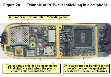
The continued miniaturisation of surface-mounted devices (SMDs) and the increasing density of PCBs, are making it more necessary to shield different zones of a product from each other, to achieve the desired levels of functional performance in the product.
The continued shrinking of the silicon features in ICs is making them more susceptible to signal degradation. PCB-level shielding is a low-cost way to enable modern ICs to operate reliably in the noisy environment inside a typical modern electronic product.
When integrating wireless (radio) communications with a product, the close proximity of very ‘noisy’ transmitting antennae tends to cause interference with sensitive circuits elsewhere in the product (analogue and digital devices can both be susceptible). The close proximity of very sensitive receiving antennae to ‘noisy’ circuits such as switch-mode converters and digital processing can reduce the range over which the wireless communication will work. PCB-level shielding is a valuable technique for wireless communications.
Many modern portable computing devices are equipped with a variety of wireless data communications (such as Bluetooth, IEEE 802.11) but have no visible antennas because they are mounted inside the product’s enclosure. The enclosure clearly cannot be shielded, and PCB shielding techniques are used instead.
Regulatory issues are also significant. As ICs’ silicon feature sizes decrease, digital and switch-mode power devices switch faster. Digital processing speeds are also continually increasing. The result is that modern electronic products are increasingly emitting significant levels at frequencies exceeding 1GHz. But the spectrum above 1GHz is increasingly being employed for personal communications, so regulatory emissions standards are moving to protect the radio spectrum up to 2.7GHz (in Europe) and beyond.
Modern product enclosures are perforated with increasingly large visual displays, connectors for numerous kinds of cables, slots for a wide variety of removable storage media, apertures for ventilation, and must be constructed with a number of joints for ease of assembly. At higher frequencies, constructional issues that were once negligible can seriously compromise shielding effectiveness (SE). PCB-level shielding-can be used to reduce the SE requirements for the overall enclosure, possibly even completely removing the need for enclosure-level shielding.
2.2 Overview of shielding at PCB level
Figures 2B and 2C provide an overview of the issues associated with PCB shielding. A five-sided conductive ‘shielding-can’ is placed over a circuit zone on a PCB, and electrically bonded by via holes in the PCB at multiple points around its perimeter to a plane layer inside the PCB (or on its bottom layer). The result is a six-sided conductive enclosure, part of which is embedded in the PCB itself.
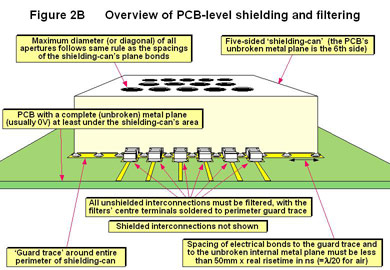

The plane layer used is usually at 0V potential, but could be at any potential. Traces that enter or leave the shielding-can must be either shielded or filtered (Figure 2B only shows filtered traces). If the plane is on an inner layer of the PCB, the traces and devices on the other side from the shielding-can are not shielded. If a circuit to be shielded has devices fitted on both the top and bottom of a PCB, both sides can be fitted with shielding-cans (and PCB plane layer may not always be required). But double-sided shielding-cans are more awkward for automated assembly.
Where the devices on the top and bottom of a PCB are associated with different circuits, they can be isolated from each other (to some degree) by using an internal PCB plane layer. It is also possible to fit shielding-cans over both of these circuit zones, each one using the same plane layer as its sixth side.
Unfortunately, when using through-hole-plate (THP) PCB construction, the plated-through holes associated with the circuits on one side of the plane layer will protrude into the shielded volume on the other side of the plane layer, where they will ‘crosstalk’ into its circuits. Also, the perforations in the common plane layer due to the clearance holes around the through-holes will reduce the SE between the top and bottom shielded volumes.
Microvia PCB technology allows the achievement of much better isolation between two shielded volumes on opposite sides of a PCB, because it uses ‘blind’ and ‘buried’ plated holes that do not pass completely through the PCB. The use of microvia PCB construction (also known as high density interconnect [6], or sequential build-up) makes it possible for plane layers not to be perforated at all. Figure 2D shows the general principle.
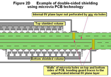
PCBs constructed using microvia technology can achieve very high levels of isolation between circuits assembled on opposite sides of a PCB with an unbroken internal plane layer between them.
2.3 Types of PCB shielding-can
Traditionally, PCB shielding-cans have been made of sheet metal, such as tin-plated steel, brass or beryllium copper. They had multiple pins around their perimeter for soldering into plated through-holes, and they usually had clip-on lids so that the devices inside could be accessed. The clip-on lids used multiple spring fingers around their perimeters to help minimise the resulting ‘leaky’ shield gaps. They were also available with internal dividers that could shield two or more zones of circuitry from each other.
Surface-mounted metal shielding-cans have become readily available in recent years, and cans of up to 50mm square are successfully assembled automatically at the same time as other SMD parts. A number of alternative designs are now available (or are being developed) to reduce weight and cost. Also, shielding-cans with reduced ‘environmental impact’ are becoming available.
Metal shielding-cans without removable lids cost and weigh less, and have better SE because they have fewer apertures. Laird Technologies has a design that allows the top of the shielding-can to be removed with a ‘key’, just like opening a traditional oblong tin of sardines. To repair the shielding-can, a new metal lid with conductive adhesive is pressed onto its body.
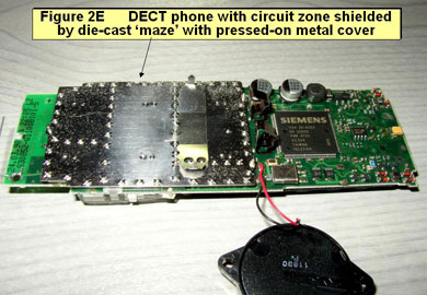
A variation on the shielding-can made from sheet metal is the die-cast metal ‘maze’ base that is soldered or press-fitted to the PCB and has metal spikes along its top edge. A flat metal lid with holes at appropriate places is pressed onto the base. An example of a PCB using this technique is shown in Figure 2E.
Plastic moulding techniques have recently become a vigorous area for research and developments. Formed plastic shielding-cans have for years been painted with conductive adhesive, or had metal layers applied by vacuum deposition (such as sputtering) or electro-plating. But the tooling costs for the automated conductive coating of such parts can be high, or they can require costly manual processing.
One alternative is to print a flat sheet of plastic with a mesh or solid layer of conductive ink, usually silver [7] [8], or to plate it with metal [9] [10]. The conductively coated sheet is then cut and thermo-formed into the desired shape. The difficulty is in designing the ink or metal film so that it can stretch enough to make a wide range of PCB-level shielding shapes without cracking, since this creates apertures and reduces the SE.
Conductively coated plastic parts can be used just as they are, if stiff enough, but some types will need mechanical assistance, such as being clipped into a plastic or metal support (often created by the internal shaping of the product’s enclosure). An alternative is to use the thermo-forms made from the conductively coated plastic sheets as ‘preforms’ for a plastic moulding process. This is sometimes called “in-mould shielding”, with the shielding preform being moulded into the finished component, thereby avoiding the need for manual assembly.
Instead of using conductively coated plastic sheets as preforms, some companies [11] are using metal plated carbon fibres in in-mould shielding processes. (Note that loading the plastic material used for the injection moulding process with conductive material is not very successful, as the resulting parts have non-conductive resin-rich surfaces.
2.4 Attaching shielding-cans to PCBs
Traditional through-hole metal shielding-cans are often soldered to their ‘sixth side’ plane in the PCB using manual methods. Wave soldering can be used in volume manufacture, but the thermal inertia of the metal shielding-cans add to the difficulties of setting up the process.
Surface-mounted metal shielding-cans are intended for automated assembly using reflow soldering methods, and usually have patterns of small holes to aid temperature equalisation [12].
High-performance metal shielding-cans are often required to be ‘seam-soldered’ to a plane layer (or guard trace) on the top of the PCB [13]. Like other types of surface-mounted shielding-cans, larger sizes would usually employ two or more pins to locate them with appropriate through-holes in the PCB.
Soldered metal cans require holes to prevent ‘popcorning’ – thermally induced changes in their shape that weaken the solder joints. But these holes affect the SE that can be achieved, so there are performance benefits to be had by not using soldered-in metal shielding boxes.
Conductive gaskets can be used with metal or shielded plastic shielding-cans. Die-cut gaskets with double-sided conductive adhesive, or formed-in-place conductive gasket glue (usually based on silicones or epoxy resin), can be used to retain shielding-cans to the PCB – as well as electrically bonding them to the PCB plane layer used for their sixth side.
Non-adhesive conductive gaskets require some other means of retaining the shielding-can, such as a plastic clip. Some PCB shields are held in place by features in the product’s enclosure (either base or cover), and fall off when the enclosure is removed. Of course, gaskets do not always need to provide a continuous bond around the perimeter of a shielding-can wall, and dots of gasket can often be used instead.
An interesting recent development in conductive gaskets is the “Gore-Shield GS5200 thermal and electrical grounding pads” [14]. These are surface-mounted soldered components with a compliant layer of thermally and electrically conductive gasket material on their upper side. Arranged around the perimeter of a shielding-can, they not only provide electrical bonding to the sixth side’ plane layer, they also help remove heat from devices inside the shielding-can.
Another method of electrically bonding plastic shielding-cans to a PCB is to design the plastic part so that it has ‘bumps’ in its conductive surface that are individually compliant enough to ensure that each one will reliably press against appropriate traces and pads on the surface of the PCB [15]. The bumps could be the sites for form-in-place gasket dots, or they could be designed as ‘spring fingers’ requiring no gaskets. This technique needs no soldering or conductive gaskets, but requires some means of holding the part in place, as for the non-adhesive gaskets described earlier.
By using plastic materials that will withstand soldering temperatures, plastic shielding-cans can be soldered onto PCBs just like surface-mounted metal cans. They have the advantage of not requiring ‘anti-popcorning’ holes; so can be designed to provide higher SE levels.
Gore have developed what they call the “snapshot shield™” [15] [16] that uses a thermoformed plastic part post-metallised on its outside. Where it meets the PCB it has a small flange with holes in it. To assemble it to the PCB, standard ball-grid-array (BGA) solder balls are deposited on the PCB at the locations of the holes, and during soldering capillary action makes the balls ‘snap’ through the holes and make contact with the outer metal layer, whilst also retaining the shield in place. The advantage of this over regular surface mounting appears to be that since the inside of the shielding-can is insulating, it is less likely to short out components and traces by accident.
2.5 PCB shielding-can materials
PCB shielding-cans have traditionally been made from stamped, drawn or folded sheet metal, but a wide variety of alternative materials are now available (or are being developed) to reduce costs, ease assembly, or reduce environmental impact. Shielding-cans can now also be made using conductive ink printed onto a variety of substrates (e.g. plastic), meshed patterns of conductive ink on substrates, metal meshes (with or without substrates), metal films deposited onto plastic substrates, etc.
Where meshes are employed the SE will degrade above a frequency governed by the size of the apertures in the mesh. There is a complex relationship between mesh size and shape, SE and frequency [17] with larger mesh sizes giving poorer SE. Meshes for GHz shielding will almost always be less than 3mm on a side.
At frequencies above 100MHz, even metal films 1 micron thick can give high values of shielding [18], so the conductive material used is usually not important for SE. However, all practical shielding-cans have their SE limited by apertures and interconnections. These issues are described below.
2.6 Apertures and gaps in shielding-cans
Apertures in shielding-cans include seams in folded metal constructions; holes for adjusting components; holes that help prevent ‘popcorning’ during automated soldering (that would weaken the soldered joints); and the spacings between the electrical bonds between the main body of the can and the PCB plane layer on its sixth side. The apertures in the plane layer caused by the clearance holes around plated through-holes have already been mentioned.
Apertures in shields must be much smaller than the wavelength of the highest frequency for which shielding performance is required. A shield with a single aperture, that has a diagonal size of one-hundredth of a wavelength, can be expected to achieve an SE of no more than 34dB at the corresponding frequency, as shown by Figure 2F.
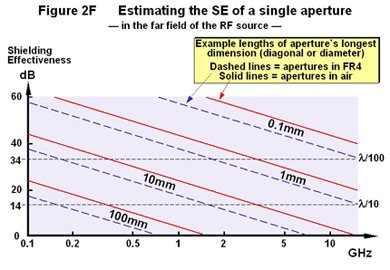
The wavelength (λ) in air of a frequency, f, is 300/f mm (when f is in GHz). The wavelength inside a PCB is about half of this, due to the dielectric constant of the PCB substrate (e.g. FR4) slowing the velocity of electromagnetic propagation to about half that of free space, within the PCB itself.
Every time the number of apertures on one face of a shielding doubles, the SE in the direction perpendicular to that face falls by up to 6dB. So if there were 8 identical apertures on one face of a shielding-can, each one having its longest dimension equal to λ/100 at the highest frequency of concern, the SE perpendicular to that face, at that frequency, should not be expected to be any higher than 16dB at the corresponding frequency.
The apertures created in the shielding-can by its electrical bonds to the inner plane layer partly lie in the air above the surface of the PCB, and partly lie inside the PCB, where the wavelength at a given frequency is about half of what it is in air. So to determine the spacing of these bonds, it is best to assume that the whole of each aperture is in the PCB material, and use a bond spacing that is half of what we would assume for apertures that were wholly in the air.
For example, if it were required to achieve 20dB of SE at 3GHz in any direction around a 50mm square shielding-can, we would firstly note that the wavelength at this frequency is 100mm in air and 50mm inside the PCB material. A single aperture of 1mm diameter in air, or 0.5mm inside the PCB, would limit the maximum achievable SE of one face of the shielding-can to 34dB, so 7 apertures should result in 20dB.
Since the shielding-can is 50mm along each side, using an electrical bond spacing to the plane layer of 0.5mm would result in 100 apertures along that edge – many more than the maximum of 7 permitted by our 20dB specification. This situation is dealt with by using a plane layer (or wide ‘guard trace’) on the same surface of the PCB that the shielding-can is to be fitted, and electrically bonding the wall of the shielding-can to that layer (or trace) along its whole length. “Seam-soldering” is the traditional way of doing this for metal cans, but conductive gaskets or conductive glue can be just as good.
Now the electrical bonds to the inner plane layer do not create apertures in the air above the surface of the PCB. But we still have a problem with the apertures created by the spacings of the via holes between the guard trace and the plane layer inside the PCB. Using normal THP PCB techniques it is difficult to space them much closer than 1mm, but waveguide-below-cutoff techniques (see below) can be used to improve their SE considerably.
2.7 Waveguide-below-cutoff methods
So far, the apertures that have been discussed were assumed to be of negligible material thickness compared with their length or width. But where an aperture’s length or width is less than one-tenth of a wavelength, increasing its thickness will reduce its ‘leakage’, improving the SE of its shielding-can.
Real benefits for SE begin to occur when the thickness of the aperture (the distance the electromagnetic fields must travel to get from the inside of the shielding-can to the outside) is comparable with the diagonal or diameter of the aperture. The cut-off frequency of a waveguide in GHz is given by 150/g where g is the longest dimension of the gap (diagonal, or diameter) in millimetres. The attenuation of a waveguide below cutoff, at a frequency below 60% of the cutoff frequency, is estimated by 27d/g dB where d is the depth of the waveguide. Figure 2G gives a few examples.
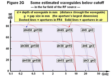
When the frequency to be shielded is above 1GHz, the apertures in the shield will usually need to be less than 3mm in air, or 1.5mm inside the PCB, and waveguide-below-cutoff techniques can be used without sacrificing too much PCB area.
In the above example of a shielding-can with an SE specification of 20dB at 3GHz, we had a problem with the spacing of the through-holes that provide the electrical bonds between the plane layer (or guard trace) on the top surface of the PCB and the plane layer that provides the sixth side of the shielding-can. If the vertical spacing between the planes (or guard trace and plane) was 1.6mm and we used a 1mm spacing laterally between the via holes, the diagonal of the resulting apertures would be about 2mm, giving a cutoff frequency around 37.5GHz (assuming a 50% velocity of propagation inside the PCB) – well beyond the 3GHz we are concerned about.
A 6mm overlap between the top plane (or guard trace) and the inner plane would achieve an SE of about 81dB for each aperture at 3GHz. The 50mm side of the shielding-can requires 50 of these 1mm wide apertures, and this quantity would reduce their overall SE by about 34dB to about 47dB. Compared with the 20dB SE specification this is a very good figure, showing how effective the waveguide-below-cutoff technique is.
Note that the waveguide-below-cutoff created by the plane (or guard trace) on the top surface plus the layer providing the sixth side of the shielding-can, can extend inside or outside its wall, or lie partially inside or outside.
As well as the waveguide-below-cutoff technique being used inside the PCB, it can be used to reduce the effects of apertures in the rest of the shield can. It is important to note that no conductor should be routed through a waveguide-below-cutoff aperture – to do so would reduce its SE to zero.
2.8 Near field effects on shielding
The above discussions and Figures assumed that the fields to be shielded from were all ‘far fields’ (sometimes called plane waves) – and this is usually the case when designing a shielding can for protection against the RF fields generated during an immunity test (e.g. when testing according to IEC 61000-4-3).
But when the apertures are in the ‘near field’ regions of the sources (are within one-sixth of a wavelength at the frequencies of concern) the SE is very much less that that calculated assuming far field conditions [25]. The near field is the normal situation when using a PCB mounted shielding can to reduce the emissions from devices or the traces associated with them.
Determining the SE of a shielding can with apertures that are in the near field requires sophisticated computer simulation using modelling software that has been calibrated for such purposes (tested and proved against real-life measurements). Alternatively, simple test set-ups can be created and tested in a laboratory well in advance of PCB layout (e.g. using simple loop and wire antennas driven from a signal generator).
However, the results in [25] point to three design guides:
a) If the SE for a device or trace is to be 40dB or more, keep the spacing between the device/trace and the shielding can’s apertures >> 2L, where L is the longest dimension of the apertures.
b) Minimise all aperture dimensions
c) Space the apertures as far apart from each other as possible
When using THP PCB technology, the PCB plane that generally forms one side of a shielded enclosure on a PCB is almost always perforated with ‘antipads’ (clearance holes) around numerous via holes. These antipads are typically 1mm or so in diameter, and of course are very close to other traces and PCB-mounted devices, so will limit the maximum attainable SE as far as emissions are concerned, even when the shielding can has no apertures and is seam-soldered to a top-side plane.
For the best PCB shielding, unperforated planes are required, and this means using HDI (microvia) PCB technology instead of THP, and this is discussed in Part 7 of this series.
2.9 Cavity resonances
Resonances (standing waves) can occur within the cavity formed by a shielding-can at frequencies at which whole numbers of half-wavelengths will fit between its sides. They can be calculated (in GHz) by:
f = 150 √ {(l/L)2 + (m/W)2 + (n/H)2}
– where: l, m, n are integers (0, 1, 2, 3, etc.) and L, W, H are the box’s length, width, height (in millimetres) respectively. Usually we are most interested in the lowest resonant frequencies of the longest dimensions, when l = 1, m = 0, n = 0 (when the general equation simplifies to: f = 150/L), or when l = 0, m = 1, n = 0 (when the general equation simplifies to: f = 150/W). For example, a 50mm by 30mm box will have its lowest resonant frequencies at 3GHz and 5GHz, in its length (L) and width (W) directions respectively.
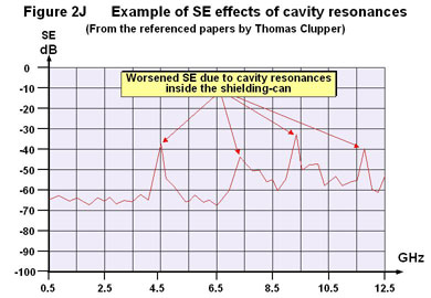
Resonances inside shielding-cans cause local amplification of their internal electric and magnetic fields at ‘hot spots’ within the shielding-can, and these increase the coupling between circuits covered by the same shielding-can. Figure 2H shows the coupling measured inside one example of PCB shielding-can [15] [16].

Also, the SE of a shielding-can is reduced at its internal resonant frequencies, with 20dB reduction being recorded by [15] [16]. This reduction in SE appears to be due to locally intense fields (hot spots) being near to apertures and conductor penetrations, causing them to leak more. Figure 2J shows the SE of the same PCB shielding-can that was measured for Figure 2H.
So it is best to use shielding-cans that have length and width dimensions much smaller than half a wavelength at the highest frequency of concern, to prevent internal resonances from occurring in the frequency range concerned. Multiple shielding compartments can be formed in one shielding-can component to increase resonant frequencies, and also to help reduce interaction (crosstalk) between circuits [16].
If it is not practical to avoid shielding-cans that are resonant within the frequency range of concern, then square (and cube) shaped structures should be avoided – as should structures with simple relationships between length, width and height (for example: 3:2:1). This is because at some frequencies such shapes will suffer from resonances due to their length and width together (or any two or three of the dimensions L, W and H). The amplification of internal fields at hot spots at these frequencies will be especially intense, and more likely to lead to undesirable results.
Ratios between L, W and H should ideally be irrational numbers, such as π (1.414….etc.) or the ‘Golden Mean’ (1.618….etc.), to help prevent coincidence of resonances. It will also help if the opposing sides of the shielding-cans are not parallel, but this technique is not often used, maybe because it does not result in a very pleasing appearance for a PCB assembly.
Another useful technique where cavity resonances in a shielding-can are potential problems is to use microwave-absorbing materials, such as Q-Zorb from Laird Technologies [18]. These are elastomers loaded with ferrite particles, usually a millimetre or two thick, glued to the inside of the lid of a shielding-can. These convert magnetic fields into heat, thereby damping down both the electric and magnetic field resonances within the shielding-can.
3 Interconnections and shielding
If the SE of a shielded volume is not to be degraded, all of the conductors penetrating its boundaries must either be shielded or filtered.
Where a conductor is shielded, their shield must bond along the full perimeter of its interpenetration with the shielded volume. Since we are discussing shielding on a PCB – traces are shielded if they run between two plane layers that bond to all of the via holes around the perimeter of the shielding-can. These two plane layers must be electrically bonded together with plated-through via holes, and it is recommended that these vias should be no more than λ/30 apart (for example, no more than 10mm for frequencies less than 1GHz), preferably much closer.
Where a shielded cable enters or leaves a PCB shielding-can, its connector or gland must make a direct electrical connection all around the perimeter of its aperture in the shielding-can, and also all around the perimeter of the cable’s shield. This is sometimes known as 360° shield bonding. Shielding is best thought of like plumbing with copper pipes – joints must either be 360° soldered or use compression joints that achieve 360° metal-to-metal contact. Plumbing that falls short of this will leak water, and shielding that falls short of this will leak radio frequency energy and so reduce SE.
It is possible to make a fully shielded PCB assembly, using plane layers on the top and bottom of the PCB, stitched together with a ‘via wall’ all around the perimeter of the PCB, plus fitting shielding-cans over all the exposed devices and traces. Of course, such a PCB will only employ 360° shielded off-board interconnections.
3.1 Combining PCB shielding with filtering
Where a conductor is filtered, its filter must be located with its midpoint aligned with the point of the conductor’s penetration of the shielded volume, so that its input and output terminals lie either side of the shield – one terminal inside the shielding-can, and one outside.
Also, the radio frequency reference voltage (often called the ‘ground’) of the filter must be the shield’s surface at the point of the conductor’s penetration. So-called ‘feedthrough’, or ‘through-bulkhead’ filters are required. Leaded feedthrough filters are traditionally used, but require manual assembly. Modern automated assembly requires the use of surface-mounted devices (SMDs), such as those shown in Figure 2K.

Leaded feedthrough filters are screwed or soldered into appropriately dimensioned holes in the shielding-can. But SMD types lie flat on the PCB and protrude through small apertures in the bottom edge of the shielding-can’s wall, as shown in Figure 2B. The holes for the filters are known as ‘mouseholes’, for reasons that are obvious to anyone familiar with ‘Tom and Jerry’ cartoons.
Figure 2L shows that the filters’ centre terminals must be soldered to the guard trace that follows the perimeter of the shielding-can. Each feedthrough filter must be symmetrically placed with respect to the via holes on each side of it (the vias link the guard trace and the wall of the shielding-can to its sixth side PCB plane).
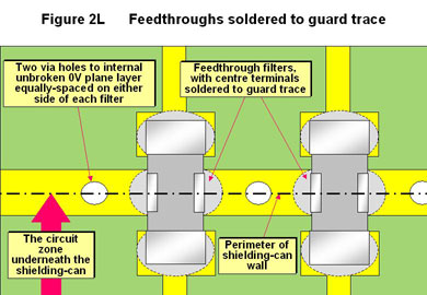
Figure 2M shows the very beneficial effect of the shielding-can on the filtering performance of an SMD feedthrough filter. Such filters need to be combined with a shielding-can to achieve any significant filtering performance at frequencies above 1GHz.
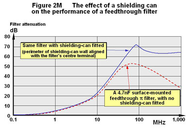
Figure 2N shows how a device (such as an A/D converter, opto-coupler, CM choke or filter array) might cross the boundary of a shielded zone. Of course, as sketched, the device is of the type that has all of its input pins along one side, and all of its output pins along the other, so that it can be placed so as to ‘straddle’ the 0V guard trace (and have a mousehole cut in the shielding-can to go over it).
Devices for which the pins are not so conveniently arranged can be more difficult to employ successfully on high-performance PCBs or PCBs with advanced EMC characteristics – so the pinout of such ‘zone interconnecting’ devices should be made an important consideration when selecting devices early in a project.
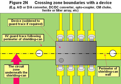
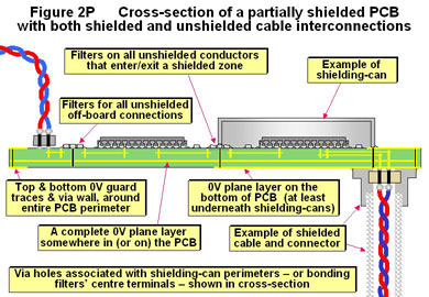
Figure 2P sketches the construction of a PCB assembly that is shielded and filtered. In some circumstances such an assembly might not need any further EMC measures, apart from a plastic box or other means to prevent electro-static discharges occurring directly to its unshielded components.
Sometimes adequate EMC performance can be achieved solely by the use of the filters or shielding-cans. It may be worthwhile experimenting, during EMC testing [19], with lower-cost three-terminal filters, feedthrough capacitors, ferrite beads, or even zero-ohm links – so it helps to ensure that the pad patterns for the filters will accommodate a variety of such devices.
4 Combining shielding with heatsinking
Some modern ICs dissipate significant amounts of heat, and require heatsinking. Where PCB-level shielding is also required, shielding-cans are combined with heatsinks. The metal base of the heatsink becomes the lid of the shielding-can, so the shielding-can on its own is little more than a four-sided shielding wall – with its bottom face completed by a PCB plane layer – and its top face completed by the base of the heatsink. Figure 2R shows a cross-section of an example based on a spring-finger type of ‘picture frame’ shield that is simply held in place by the heatsink (it will probably need a couple of locating pins with matching holes in the PCB). The clip or other construction that holds the heatsink in place is not shown.
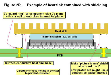
The base of the heatsink must have a highly conductive surface using metals chosen so that they will not corrode after years of contact with the shielding wall. The heatsink is usually not soldered to the shielding wall (although this could be done under certain circumstances). Normally, all the various ‘pressure sensitive’ techniques that can be used for attaching shielding-can walls to PCBs can also be used to electrically bond the walls to the base of the heatsink. The spacing rules for the electrical bonds between the shield wall and the base of the heatsink are the same as those (above) for bonds between the shield wall and the PCB’s 0V guard ring and internal unbroken plane, the 6th side of the shielding volume.
5 Environmental issues
Two European Directives concerning the protection of the environment (known as WEEE and RoHS) will come into force in the European Union in 2006, with at least one other (known as EuPD) planned before 2010. The RoHS Directive will ban the use of tin-lead solder, and most people will go for tin soldering instead which may effect the choice of components available for use in filtering. But both of these directives will influence the type of shielding used, and the materials used in shielding-can construction.
The volatile chemicals used in some conductive coating and electro-plating processes have a negative environmental impact, and these processes tend to make the coated materials difficult to recycle [20]. Vacuum metallisation is claimed to be more ‘eco-friendly’, and tin and aluminium are non-toxic and easy to recycle. So vacuum metallised plastic shielding-cans (employing tin or aluminium) that are pressed, clipped or soldered into place, may have fewer environmental disadvantages than some other plastic shielding techniques. Thermo-formed shielding inserts aid the recycling of plastic enclosures [8]. Surface-mounted metal cans are easy to remove and recycle [12].
6 PCB-level filtering
6.1 Reasons for filtering on the PCB
The reasons for filtering at PCB level are very similar to those described in section 2.1 for shielding at PCB level, and will not be repeated here.
Section 1 above said that shielding and filtering work together to create high-performance segregation. High levels of shielding will not be achieved without filtering, and high levels of filtering will not be achieved without shielding, especially at frequencies above 100MHz (made especially clear by Figure 2L above). So it is important to note that as problem emissions and immunity frequencies continue to increase and go beyond 1GHz, and as pressure on costs and timescales continues to increase, careful design of PCB filtering will increasingly be required.
6.2 Overview of PCB filtering
General filtering issues are described in Part 3 of [1]; Part 3 of [2]; Volume 2 of [5] and Chapter 8 of [21]. PCB filtering employs the same general design, but issues and design details more relevant to advanced PCB segregation are described in this section, and section 7 below.
A number of basic single-line single-stage filter types are available…
• series resistor (R) or series inductor (L)
• shunt capacitor (C)
• resistor-capacitor (RC) or inductor-capacitor (LC)
• resistive Tee (RCR) or inductive Tee (LCL)
• capacitor-resistor (CR) or capacitor-inductor (CL)
• resistive Pi or π (CRC) or inductive Pi (CLC)
When filtering frequencies above a few MHz, soft ferrite ‘suppresser’ ferrites are generally used instead of inductors, although they are shown on schematics by the same symbol.
Common-mode (CM) noise is usually the major cause of high emissions and poor immunity between 1MHz and 1GHz. When filtering more than one conductor, CM chokes wound on a soft-ferrite cores generally provide better attenuation of RF CM noise than a row of individual soft ferrites, so it is best to layout PCBs so that selected CM chokes can be fitted instead of a row of individual resistors or ferrites (see Figure 2S below), double-padding if necessary. If it turns out that a CM choke is necessary (although, due to its higher cost, it was hoped that it wouldn’t be) this little bit of forethought will save the many weeks delay and the cost of a board ‘respin’.
The above filter types can be combined together to create multistage filters with greater attenuation. For EMC use, most low-power DC, analogue and digital signal filters rarely seem to need to use more than a single stage filter. But filters for equipments’ AC supplies (mains inputs) and filters for pulse-width modulated (PWM) and other semiconductor power controlled outputs may need to use multi-stage filters to pass regulatory or contractual EMC tests.
Section 6.4 below describes PCB layouts for all low-power DC, analogue and digital signals that enter or leave a PCB via ‘off-board’ cables. Similar design considerations apply to all filters used on traces between circuit zones within a PCB (e.g. Figures 2, 11, 12, 13 and 14) except that the 0V plane should never be gapped or split except as part of an overall EMC plan carefully-designed by a PCB EMC expert.
Gaps and splits in planes are discussed in Part 4 of this series (in a future issue of this Journal), so this issue will not be discussed here, expect to say that gapping and splitting planes was a good idea twenty years ago when most problem frequencies lay below 200MHz, but these days it is generally a very bad idea. Unfortunately most of the application notes for microprocessors, A/D and D/A converters, codecs and the like still seem to be stuck in a ‘traditional’ rut and recommend gapped and split planes despite the significant signal integrity and EMC benefits provided by ‘solid’ (unbroken) planes.
6.3 High-performance filtering requires a good quality RF reference
PCB shielding-cans require an unbroken internal metal plane layer as their 6th side. An unbroken internal metal plane layer also makes a high-quality RF reference for a filter, without which filtering performance will suffer.
We can see that the provision of an unbroken plane layer (usually the 0V plane) allows the implementation of advanced PCB segregation techniques (using shielding and filtering), as well as the many other PCB EMC benefits which will be described in Part 4 of this series (in a future issue of this Journal).
6.4 Design of single-stage low-power and signal PCB filters
In general – where all the items of interconnected equipment are not referenced to large plates of well-bonded metal (as they are in a typical warship or submarine) – the best type of filtering for an unshielded off-board connector/cable has a series resistor or soft ferrite suppresser as its final component before the off-board conductor. An example of a PCB layout for an unshielded off-board connector, using RC or LC filtering with low-cost two-terminal capacitors, is shown in Figure 2S. (Multi-padding so that CM chokes can be used instead of resistors or ferrites is not shown in this Figure.)
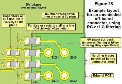
Aligning filter components in rows
Figure 2S shows how the ferrites connected to the off-board connector/cable are arranged all in a neat row. This layout detail is most important to optimise the attenuation of these devices at frequencies above 100MHz. Due to the connection density of some modern connectors, it is tempting to stagger the layout of the resistors or ferrites, but this should never be done. Staggering the layout of the ferrites increases the stray capacitive coupling between their filtered and unfiltered terminals – it may not seem like very much extra capacitance but it can be enough to entirely negate their filtering effect.
If achieving a single neat row of resistors or ferrites is impossible, then either smaller ferrite components (0402 sizes are becoming increasingly available) or integrated ferrite arrays should be used, or else the ferrites should be arranged on both the top and bottom of the PCB – with the top row placed exactly above the bottom row.
Arranging the series resistors or ferrites in a row is also necessary to assist with fitting a CM choke instead, if one is required. The input and output connections for a CM choke should always be kept well apart from each other.
The RC or LC filter capacitors are also arranged in a neat row behind the row of resistors or ferrites, with their 0V ends via’d to the unbroken internal 0V plane layer using the shortest fattest traces possible (to minimise their series inductance and improve the capacitor’s high-frequency performance). Via-in-pad techniques are preferred for the 0V terminals of the filter capacitors – easy to achieve when using micro-via PCB techniques (which will be discussed in Part 7 of this series, in a future issue of this Journal) or wave-soldered PCBs. It is generally held that via-in-pad techniques cannot be used with reflow soldering, but some PCB fabricators seem able to achieve this without increased costs and with good yields.
Filtering the off-board ‘GND’ conductors
The ‘GND’ connections in the connector/cable are also fitted with pads for ferrites, because it often helps to fit the same type of ferrites in an off-board 0V connection as are fitted in the signal paths. If a CM choke is required it must have all of the off-board conductors routed through it at once (or at least each signal plus its dedicated return conductor in a number of CM chokes), so providing suitable pads for the GND signals will help.
Cutting back the 0V plane
Figure 2S shows the 0V plane cut back over part of the filter’s area – in fact it is cut back just as far as the ‘circuit side’ terminals of the resistors, ferrites or CM chokes. This is done because the proximity of the 0V plane to the connector/cable terminals of these components increases their stray capacitance and reduces their filtering performance at high frequencies. Cutting back the 0V plane as shown also helps to prevent unwanted coupling between the noises in the external conductors and the PCB’s reference 0V plane. Sometimes it may be better not to cut back the 0V plane, even though this would compromise the performance of the series resistors, ferrites or CM chokes, as discussed in Section 7.
All of the examples in this section have series resistors; ferrites or CM chokes as their final filter components before the connector/cable. Other types of filters (e.g. Pi) that connect the connector/cable conductors directly through a capacitor to the 0V plane should not use a cut-back 0V plane – the plane should extend right to the edge of the PCB and be ‘webbed’ around the connector/cable connections as described in Part 4 of this series (in a later issue of this Journal).
No other traces or components in the ‘Connector Zone’
A dotted area is shown in Figure 2S, called the “Connector Zone”. This is the zone of the PCB dedicated solely to the filtering of off-board (external) conductors. Stray capacitance and mutual inductance between the filter’s components and traces in this zone can completely ruin the filtering provided for the off-board connector/cable – so no other traces, components or power planes are permitted in this zone, on any layer of the PCB – even if the 0V plane is not cut back as described above.
Shielding the connector zone
The “Connector Zone” would be the area covered by a shielding-can, if shielding was found to be necessary (as it might be). Such shielding would be designed according to the sections on PCB shielding-cans above – but in the case of an off-board connector/cable filter zone it would have an open side for the connector or cable.
Where a metal (or metallised plastic) connector panel is used, the open side of the connector zone’s shielding-can must make a multipoint electrical bond to the inside surface of the connector panel – usually best achieved (for low-cost assembly) with a suitable type of conductive ‘EMC gasket’. Even if it is hoped to use a plain plastic enclosure for the PCB with no enclosure shielding, it is still best to design so that metal plated or conductively painted plastic can be used, or else an internal metal foil can be applied, bonded at multiple points to the PCB’s unbroken internal 0V plane as described in Part 3 of this series (in a future issue of this Journal).
Using shielding to improve filter performance
The performance of the series resistors, ferrites or CM chokes shown in Figure 2S would be improved if the wall of a PCB shielding-can were aligned with the cut-back edge of the 0V plane, so that the resistors or ferrites protruded through mouseholes in it. The design of the shielding-can would follow Sections 2 and 3 above.
Where a shielding-can was already fitted over the whole connector zone, it should include an internal wall splitting it into two compartments. This internal wall is the one that aligns with cut-back edge of the 0V plane and has the mouseholes for the resistors or ferrites.
Where there is no shielding-can fitted over the whole connector zone, then the shield wall that is used to improve the performance of the series resistors or ferrites could be part of a shielding-can that included the ‘PCB side’ of the filter’s circuitry (maybe also covering other circuit zone), or part of a connector/cable shielding-can that is bonded to the connector panel as described above.
Tee filtering
Figure 2T shows how the ‘design rules’, described in detail for Figure 2S above, apply to a Tee filter. The connector zone for this filter type extends to cover at least half of the series resistors or ferrites on the circuit side of the filter. Mouseholed shielding-can walls to improve filter performance could be fitted along the centre of either of the rows of series resistors, ferrites or CM choke(s); or along the row of capacitors. Even better filter performance could be achieved by fitting shielding-can walls along any two, or even all three, rows of filter components. If only one such mouseholed wall was to be used, it would be best located along the row of capacitors.

Figure 2U shows a variant on the Tee filter of Figure 2T, this time using three-terminal capacitors to achieve better filtering at frequencies above 300MHz. Whenever using three-terminal filters a 0V guard trace is required for soldering their centre terminals to, and there should always be two 0V via holes equally spaced on either side of each device to improve their high-frequency performance. The provision of mouseholed shielding-can walls to improve filter performance follows the design rules of Figure 2T, but a wall aligned with the capacitors should follow their 0V guard trace and be electrically bonded to it according to the Sections 2 and 3 above.
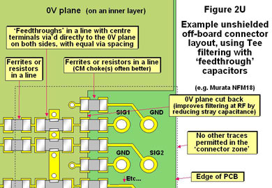
Figure 2V shows an alternative higher-performance circuit design and PCB layout to Figure 2T, and it could also be an improvement on Figure 2U (depending on the application). The two current loops associated with the input and output of a Tee filter both share the same capacitor, and there is inevitable magnetic flux coupling between them that degrades the filter performance. This would be true even if there were no partial inductances in the capacitor, its traces or via holes (which, of course, there always is). Figure 2V reduces this coupling by using two half-value capacitors spaced far apart, so that the current loop associated with the filter’s input circuit couples less magnetic flux with its output circuit.
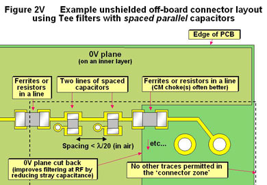
The maximum spacing between the two half-value capacitors in Figure 2V is λ/20 (using the λ values for propagation in air, in FR4 it would be λ/10) at the highest frequency to be filtered; otherwise the current loop between the two capacitors becomes resonant, reducing its benefit.
Figure 2X shows the correct use of an integrated Tee filter, such as the Murata NFE31 series. Integrated Tee filters are three-terminal devices and their centre terminals must be soldered directly to a 0V guard trace as was also shown in Figures 2B and 2L in Sections 2 and 3 respectively, and Figure 2U. Don’t forget that there should be two 0V via holes equally spaced in the guard trace on either side of each filter.
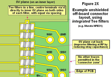
Where it is desired to use mouseholed shielding-can walls to improve the performance of Figure 2X’s filter, it should follow the 0V guard trace and be electrically bonded to it according to the Sections 2 and 3 above.
Figure 2Y shows the use of an IC-style integrated filter. IC filters can be arrays of ferrites, RC, LC, Tee or Pi filters, and their main benefit is that they save PCB space. Resistive RC, Tee, and Pi filters are becoming available made using silicon IC processes (e.g. from California Micro Devices), and this is sometimes claimed to improve their filtering performance at frequencies above 300MHz due to the lower inductances associated with their internal capacitors. It is not obvious where to fit a mouseholed shielding-can wall over an IC filter, so in the absence of any other information it should follow the centre line of the device.

The use of integrated filters such as those shown in Figures 2X and 2Y provides less filter choice than discrete filter components such as those shown in Figures 2S, 2T, 2U and 2V, but the PCB space required can be much less so the compromise may be acceptable.
6.5 Power filtering on PCBs
AC supply (mains) and similar high-power filters should follow the same design considerations as described in section 6.4 above, making suitable allowances for the increased size of the components.
SAFETY NOTE: It is very important to correctly design all of the safety aspects of such filters, such as creepage and clearance distances, leakage currents in the protective (earth/ground) conductor, the use of safety approved parts, etc.) – for more on this refer to Volume 4 of [5].
6.6 Filtering for shielded connectors
When using shielded off-board connectors/cables having 360° shield terminations to the unbroken 0V reference plane in the PCB – and at the other end of the cable (see: Part 4 of [1] or [2]; Volume 2 of [5]; Chapter 8 of [21] or Chapter 6 of [22]) – then filters may not be needed at all. If filters are employed they will generally employ capacitors, or RC, LC, or Pi types with the connector/cable conductors firstly connected via a capacitor to the 0V plane, and the 0V lane will not be cut back in the vicinity of the connector.
7 Placement of off-board interconnections
All of the off-board conductive interconnections (e.g. cable connectors) should ideally be located along one edge of the PCB, close together, with no active circuitry located between them. It may be that EMC improvements can be achieved by locating the off-board connectors on two adjacent sides of a PCB, as close as possible to one corner. The purpose of this placement strategy is to minimise the CM potential differences between the off-board conductors, which is a direct cause of emissions.
The provision of a single unbroken 0V plane (often called a reference plane or RF reference plane) in a PCB – plus ensuring that each off-board conductor is electrically bonded to that 0V plane (directly or capacitively) – is an extremely powerful technique for reducing the emissions from off-board conductors. It is described in more detail in Part 4 of this series (in a future issue of this Journal).
Nevertheless, despite the very low partial inductance of such reference planes, the increasingly high frequency currents flowing in them as a result of the use of modern silicon devices can cause significant noise potential differences between one part of the plane and another. If conductors enter or exit the PCB at locations suffering from differing plane noise voltages, they will tend to behave as ‘accidental antennas’ and radiate the plane noise, thereby increasing the board’s emissions. This is the reason for the ‘connector placement rule’ described above.
If for some reason the off-board connectors have to be placed far apart, or have active components located in areas of the PCB between them, it may be a better compromise not to cut back the 0V plane in the connector area. This would trade off a reduced performance for the filter (see 6.4) with an improved plane inductance for lower CM noise due to plane noise. It is almost impossible to predict which will be best, so experiments with each design may be required to find the best compromise.
8 Compromises
It is easy to write an article like this and simply list all of the relevant good EMC design techniques, but in real life there are a great many design trade-offs (compromises) to be made, and this is where the circuit and PCB designers really earn their keep. It is very important for a designer to know all of the compromises he/she is making, and their costs and benefits, to avoid accidentally neglecting an important issue that will cause unplanned costs or delays later in a project – when the true costs of changes are much higher than the same changes made early in a design project, see Figure 1A of [23].
Where any of these “Advanced PCB Design Techniques for EMC” cannot be employed, appropriate problems with EMC must be expected. If the problems are not found to arise on the current project, this does not mean they can be neglected. They will arise on the next project, or the one after that, due to the continuing shrinking of the silicon feature sizes in all transistors and ICs [23] and the increasing density of electronic components on PCBs.
The EMC problems caused by neglecting these techniques might manifest themselves as increased development time, poor yield in serial manufacture, difficulties in commissioning custom-designed equipment, failure to meet regulatory compliance standards, or increased levels of warranty returns, all with their associated damage to company profitability.
So at least use this article as a checklist, and ensure that – where each of its recommendations are not followed – this was a cost-effective technical compromise based on all of the facts. If it is not obvious whether a compromise is acceptable or if it will create more problems than it saves, experiments are recommended at an early stage in the project. EMC experiments might not need to employ EMC test labs or IEC/EN test methods – quite often the relative performance of two options can be judged using the low-cost and quick ‘development’ test methods described in [24].
9 References
[1] Keith Armstrong, “Design Techniques for EMC” (in six parts), UK EMC Journal, Jan – Dec 1999
[2] Keith Armstrong, “Design Techniques for EMC” (in six parts), http://www.compliance-club.com/KeithArmstrongPortfolio
[3] M K Armstrong, “PCB Design Techniques for Lowest-Cost EMC Compliance: Part 1”, IEE Electronics and Communication Engineering Journal, Vol. 11 No. 4 August 1999, pages 185-194
[4] M K Armstrong, “PCB Design Techniques for Lowest-Cost EMC Compliance: Part 2”, IEE Electronics and Communication Engineering Journal, Vol. 11 No. 5 October 1999, pages 219-226
[5] “EMC and Electrical Safety Design Manuals”, a set of four volumes edited by Keith Armstrong and published by York EMC Services Ltd., 2002, ISBN 1-902009-07-X, sales@yorkemc.co.uk, phone: +44 (0)1904 434 440.
Volume 1 – What is EMC? ISBN 1-902009-05-3
Volume 2 – EMC Design Techniques – Part 1
ISBN1-902009-06-1
Volume 3 – EMC Design Techniques – Part 2
ISBN 1-902009-07-X
Volume 4 – Safety of Electrical Equipment
ISBN 1-902009-08-8
[6] The basic standard on microvia PCB technology is IPC-2315, from the Institute of Printed Circuits at http://www.ipc.org.
[7] Steve Owen, “The Shielding Effectiveness of In-Mould Labelled Enclosures”, EMC York 2000 Conference, 10-11 July 2000, http://www.yorkemc.co.uk
[8] Chris Hills, “Formed EMI Shields, the Green Replacement for Conductive Paint and Plating for Plastic Housings”, EMC Compliance Journal, June 2000, pp 36-39, http://www.compliance-club.com
[9] Maria Sabrina Sarto et al, “New Light-Weight Formable Shields”, EMC Compliance Journal, Aug. 2001, pp 17-19, http://www.compliance-club.com
[10] Maria Sabrina Sarto et al, “An Innovative Shielding Concept for EMI Reduction”, IEEE EMC Society Newsletter, Summer 2001, Issue No. 190, pp 22-28
[11] “EMC Shielding with Carbon Fibres”, IEE EMC Professional Network, EMC Industry News 2002-11-21
[12] Jack Black, “Automated Installation of Surface Mountable EMI Shields Using Tape and Reel Packaging”, BMI Inc., Palatine, IL, USA
[13] Darryl Yarborough, “EMI Shield Mounting Methods, Some Tried and Some New, Through-Hole, Surface, and the New Hybrid”, Conformity, Jan. 2001, pp 32-34, http://www.conformity.com
[14] Gore-Shield GS5200 Gaskets, http://www.gore.com
[15] Roy Bjorlin, Gary Shawhan, “Conformal Board-Level Shielding Products”, Interference Technology Annual Guide 2003, pp 226-230
[15] Thomas Clupper, “Improve PCB Shielding for Portable Devices”, Microwaves and RF, May 2003, pp 72-84
[16] Thomas Clupper, “A New PCB-Level Shielding Technology”, Interference Technology Annual Guide 2003, pp 187-195
[17] Eis