Advanced PCB design and layout for EMC Part 5 - Decoupling, including buried capacitance technology (Second Part)
This is the second part of Keith Armstrong’s article that appeared in Issue 55, EMC & Compliance Journal, November 2004. Due to its length we had to split it between the two issues. This issue contains Section 3 - Decoupling with 0V/Power plane pairs, onwards.
This is the fifth in a series of eight articles on good-practice design techniques for electromagnetic compatibility (EMC) for printed circuit board (PCB) design and layout. This series is intended for the designers of any electronic circuits that are to be constructed on PCBs, and of course for the PCB designers themselves. All applications areas are covered, from household appliances; commercial, medical and industrial equipment; through automotive, rail and marine to aerospace and military.
These PCB techniques are helpful when it is desired to…
- Save cost by reducing (or eliminating) enclosure-level shielding
- Reduce time-to-market and compliance costs by reducing the number of design iterations
- Improve the range of co-located wireless datacomms (GSM, DECT, Bluetooth, IEEE 802.11, etc.)
- Use very high-speed devices, or high power digital signal processing (DSP)
- Use the latest IC technologies (130nm or 90nm processes, ‘chip scale’ packages, etc.)
The topics to be covered in this series are:
- Saving time and cost overall
- Segregation and interface suppression
- PCB-chassis bonding
- Reference planes for 0V and power
- Decoupling, including buried capacitance technology
- Transmission lines
- Routing and layer stacking, including microvia technology
- A number of miscellaneous final issues
A previous series by the same author in the EMC & Compliance Journal in 1999 “Design Techniques for EMC” [1] included a section on PCB design and layout (“Part 5 – PCB Design and Layout”, October 1999, pages 5 – 17), but only set out to cover the most basic PCB techniques for EMC – the ones that all PCBs should follow no matter how simple their circuits. That series is posted on the web and the web versions have been substantially improved over the intervening years [2]. Other articles and publications by this author (e.g. [3] [4] and Volume 3 of [5]) have also addressed basic PCB techniques for EMC. This series will not repeat the basic design information in these articles – it will build upon it.
Like the above articles, this series will not spend much time analysing why these techniques work, they will focus on describing their practical application and when they are appropriate. But these techniques are well-proven in practice by numerous designers world-wide, and the reasons why they work are understood by academics, so they can be used with confidence. There are few techniques described in this series that are relatively unproven, and this will be mentioned where appropriate.
Table of Contents, for this Part of the series
Section 1 and 2 are contained in Issue 55, November 2004.
1 Introduction to decoupling
2 Decoupling with discrete capacitors
2.1 Which circuit locations need decaps?
2.2 The benefits of decaps in ICs and MCMs
2.3 How much decoupling capacitance to use?
2.4 Types of decaps
2.5 Layouts that reduce the size of the current loop
2.6 Series resonances in decaps
2.7 Using ferrites in decoupling
2.8 Splitting the decap into two
2.9 Using multiple decaps in parallel
2.10 Other ways to reduce decap ESL
In this issue:
3 Decoupling with 0V/Power plane pairs
3.1 Introduction to the decoupling benefits of 0V/Power plane pairs
3.2 The distributed capacitance of a 0V/Power plane pair
3.3 PCB 0V and power routing with 0V/Power plane pairs
3.4 Defeating parallel decap resonances when using 0V/power plane pairs
3.5 ‘Cavity resonances’ in 0V/power plane pairs
3.6 Bonding planes with decaps to increase resonant frequencies
3.7 Power plane islands fed by π filters
3.8 Damping cavity resonance peaks
3.9 The spreading inductance of planes
3.10 The 20-H rule
3.11 Taking advantage of decap series resonances
3.12 Decap walls
3.13 Other 0V/Power plane pair techniques to reduce emissions
3.14 The buried capacitance technique
4 Field solvers for power bus impedance simulations
5 EMC-competent QA, change control, cost-reduction
6 Compromises
7 References
3. Decoupling with 0V/Power plane pairs
3.1 Introduction to the decoupling benefits of 0V/Power plane pairs
It was mentioned in section 2.5 above that placing 0V and power planes areas on adjacent layers significantly increases the mutual inductance between them. Since the current flows in each plane are equal and opposite, this mutual inductance reduces the decaps’ interconnection inductances, which is a very good thing. Closer spacing between the two planes means higher mutual inductance and lower decap interconnection inductances.
Another consequence of having 0V and power planes in close proximity on adjacent PCB layers (known as a 0V/Power plane pair) is that they create a distributed capacitance – and this can be used as an embedded decoupling capacitance to help achieve a low impedance power bus at frequencies up to many GHz.
The use of large power planes to create useful amounts of embedded, distributed decoupling capacitance is the main topic of this section. As far as the propagation of the wanted digital and analogue signals is concerned, a power plane is a copper sheet just like a 0V plane, so all of the general issues about planes, especially when signals are routed near to, or cross, their edges applies in just the same way – and the guidance in [7] (especially its section 4) applies equally to power planes.
Some EMC experts prefer not to use power planes, because if not used carefully the cavity resonances that naturally arise when they are used in combination with another plane can cause an increase in emissions. This section will show how power planes can easily be used to reliably achieve a net overall EMC benefit.
3.2 The distributed capacitance of a 0V/Power plane pair
It is very difficult to achieve a low power bus impedance above 500MHz using discrete decaps mounted on a PCB, see Figures 5G, 5L, 5M, 5N and 5Q. The best that can be done in this frequency range is to place so many decaps in parallel that their overall inductance gives a low enough impedance.
Intrinsic 0V/Power plane pair capacitance has excellent performance beyond 1GHz due to its extremely low ESL, which makes its SRF very high indeed. In fact, the SRF of a 0V/Power plane pair is so high that it is never an issue of concern. If we were to plot the impedance of 1nF of 0V/Power plane pair capacitance on Figure 5G above, it would follow the dotted line that indicates the impedance-versus-frequency performance of an ideal 1nF capacitor, even if the horizontal axis was extended to 10GHz or more.
Cplane pair = 35/d nF per square metre, for FR4 (k = 4), where
d = the interplane spacing in millimetres
Thinner interplane spacing increases the capacitance, and a spacing of 50µm (2 thousandths of an inch) achieves 770nF/sq. metre (as used by the ZBC2000 product, see below). Using 2 or more sets of 0V/Power plane pairs in parallel is a simple way to double (or more) the distributed plane pair capacitance available for decoupling.
Figure 5R shows how the low impedance at high frequencies achieved by the 0V/Power plane pair can be used in combination with voltage regulators and discrete decaps to achieve a low power bus impedance over the whole frequency range of concern.
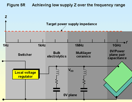
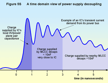
Figure 5S shows the same issue in the time domain, instead of the frequency domain.
3.3 PCB 0V and power routing with 0V/Power plane pairs
A summary of decap pad patterns for connections to 0V/Power plane pairs with brief comments on their effectiveness was given in Figure 4H of [7]. Some suitable pad patterns for connecting IC 0V and power pins to their respective planes were shown in Figure 4J of [7] and are also described in [19]. Also see Figures 5T and 5U.


Section 2.4 of [7] listed some valuable layout rules for connecting components to planes. When they are applied to the decaps and 0V and power pins of ICs, they help minimise the decaps’ interconnection inductances and allow the charge stored in the decaps to be delivered to the ICs more quickly.
Because we are trying to take advantage of the 0V/Power plane pair’s capacitance at frequencies above 500MHz, the inductance of the connection between IC and plane must be very low indeed. So it is very important indeed to connect an IC’s 0V and power pins immediately to their respective planes, as shown in Figures 5T and 5U and section 2.4 of [7]. The decaps should also be connected directly to their planes, because the interconnection inductance of the planes is much less than any trace. Via-in-pad is preferred, which can always be done for wave-soldered THP PCBs, and which some PCB assemblers can achieve using reflow-soldered THP PCBs. Via-in-pad is normal when using HDI (‘microvia’) PCB technology, see section 5 of [7] and Part 7 of this series.
The partial inductance of the length of the via holes that actually carries current between a component and a plane becomes very significant at frequencies above a few hundred MHz. (A physics purist would say that the problem was really the current loop area caused by the spacing between the component and the plane). So, to provide good power bus impedance up to and beyond 1GHz, we need to stack-up our PCBs so that they provide 0V/Power plane pairs as close to the surface-mounted components as possible, minimising the length of the via holes that must carry current.
As was mentioned in [7], the bad influence of via holes’ current-carrying lengths can be reduced by placing vias carrying equal and opposite currents very close together. Also, multiple parallel vias can be used for any current path but they must be far apart (compared with their current-carrying length) for this to be very effective. Vias with larger diameters have lower partial inductances, but (when using THP and not HDI PCB construction) larger diameter power vias make larger holes in the 0V plane and compromise its performance (see [7]), so multiple small vias are generally preferred.
Some designers have in the past preferred to ‘keep the noise out of the planes’ by using traces to connect between decaps and ICs, then connecting the decaps to the planes. The purpose of this is to avoid exciting the 0V/Power plane pair’s cavity resonances – but it is not an optimum solution because it increases the inductances in the decaps’ interconnections and prevents the full benefits of the 0V/Power plane pair’s distributed capacitance from being used.
There is no problem with noisy currents in planes providing the planes used for the power bus maintain a low impedance over all the frequencies of concern – by designing them to avoid or damp their cavity resonances. Later in this article I will describe practical low-cost methods that will achieve 0V/Power plane-based power busses that have no significant resonances over the frequency range of concern, improving the EMC (and functional) performance of the circuits on the PCB.
3.4 Defeating parallel decap resonances when using 0V/power plane pairs
Section 2 above suggested using small power plane areas to help reduce decaps’ interconnection inductance, when using multiple capacitors in parallel to reduce power bus impedance at the IC. When a power plane is extended in area to embrace all of the ICs its power bus services, and all of their decaps, we find we now have a much higher number of decaps in parallel.
When using different values of decap, as described in section 2.9 above, the use of large power planes provides so many series resonances spaced so closely together that the high impedances caused by parallel resonances are very low [14].
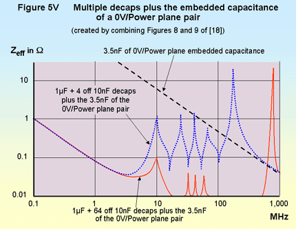
To take advantage of this, and also to help prevent cavity resonances in the 0V/Power plane pair (see below) it is recommended to place decaps all over a power plane, not just near to the ICs, no further apart than 25mm, and to minimise each decap’s overall inductance by careful layout (see Figure 4H of [7]) and careful choice of decap components. One way of looking at this approach is to say that it creates alternative low-impedance current paths nearby each high-impedance (parallel resonating) current path – so the IC’s power bus currents always can always find a low-impedance path. Figure 5V below shows an example of exactly this from UMR.
Figure 5V shows the result of some experiments at the University of Missouri-Rolla [19]. It shows that increasing the number of 10nF decaps from 4 to 64 has significantly reduced the amplitudes of most of the parallel resonances. However, the highest-frequency resonance (caused by the 0V/Power plane capacitance with its very small ESR) was not been reduced in amplitude – it was moved to a higher frequency.
An interesting observation is that when the spacing between the 0V and power planes in the pair is less than 250µm (10 thousands of an inch) the placement of the decaps with respect to their ICs becomes less critical, easing PCB layout [20].
Although Figure 5V came from an experiment that used large number of decaps all (but one) of the same value (10nF) – page 159 of [19] tells us that each capacitor had a different interconnect inductance associated with it (between 1 and 8nH). So instead of having very similar SRFs, these decaps would have had different SRFs, just as they would have had if their values were different and their interconnect inductances the same. One possible conclusion from this is that the impedance between 200MHz and the last (large) resonance would probably have been less if all of the devices had used different values but their layouts all achieved the lowest possible interconnect inductance.
3.5 ‘Cavity resonances’ in 0V/power plane pairs
Cavity resonance between 0V and power plane pairs was discussed in Part 4 of this series [7], but the implications and design issues for decoupling were left to this Part.
Achieving a low plane impedance at every frequency can be made difficult by cavity resonances (sometimes called ‘parallel plate’ resonances) – where the 0V/power plane pairs behave like unterminated transmission lines.
The natural resonant frequencies for a rectangular plane pair filled with a material with a relative dielectric constant of k are given by: fRES = (150/√k) x √{(l/L)2 + (m/W)2}
This formula gives fRES in MHz if L and W (the plane pairs’ length and width) are in metres. l and m are integers (0, 1, 2, 3 etc.) and correspond to the various modes of resonance, but it is usually only the first (lowest) resonant frequency we are most concerned with. For FR4 material (k nominally 4.0 at >1MHz) this is easily found from: f = 75/D, where D is the plane’s longest diagonal dimension (D in metres gives the frequency f in MHz, D in millimetres gives it in GHz).
For non-rectangular planes that are not simple shapes, it will usually be necessary to determine their resonant frequencies by computer simulation using field solvers, or measurement of a test PCB. But their lowest resonant frequency will still be easily estimated as 75/D MHz for FR4, where D is the plane’s longest dimension, in metres.
It is important to understand that in real life the bare-board plane resonances are significantly modified in amplitude and frequency by the presence of the electronic components and the numbers, values, types, and locations of the decaps. So the above simple analyses are only of use during a design process, and do not predict the actual resonances in a real-life power bus on a fully assembled PCB.
One way to reduce the worst effects of cavity resonances is by careful design of the planes’ shapes, and this was mentioned in [7]. This will have little effect on the lowest frequency (governed simply by the longest dimension) but it may have a useful effect on some of the higher frequency resonances.
Where the length (L) of a rectangular plane is an integer or other simple multiple of its width (W), such as 1, 1.5 or 2, the resonant frequencies of the length and width directions will coincide at some frequencies, causing higher-Q peaks (more intense resonances) at those frequencies. Murphy’s law tells us that when the clock frequency is changed just before product launch, one or more of the new harmonic frequencies will just happen to coincide with one of these more intense resonances, causing problems for EMC compliance at a time when it is very costly and time-consuming to make any changes and delays cannot be tolerated.
So it is best to avoid simple regular power plane shapes such as squares and circles, and also avoid simple L:W ratios. Ideally, choose an irrational number for the ratio of length to width of a rectangular plane. There is an infinite number of irrational numbers to choose from, but the ‘Golden Mean’ (1.618…etc… call it 1.62) gives a pleasing appearance (as Renaissance artists and ancient Greek architects knew). Thin planes should always be avoided, meaning that their L:W ratio should never be larger than 3 (or smaller than 0.33). It may also help to have non-parallel plane edges, and to avoid regular shapes such as rectangles.
Closer plane-pair spacing increases the losses in their cavity, decreasing its Q and making the cavity resonances less peaky. Closer spacing also reduces their fringing fields, reducing ‘edge-fired’ emissions. This very powerful EMC technique requires plane spacings no greater than 50µm (2 thousands of an inch). Such closely-spaced 0V/Power plane pairs are discussed in more detail in the section on “Embedded Capacitance” below.
3.6 Bonding planes with decaps to increase resonant frequencies
When cavity resonances between pairs of 0V planes was discussed in [7], it was shown that bonding them very frequently together with via holes increased the frequency at which their first resonance occurred. The idea was to ‘push’ the first resonance to such a high frequency that it was no longer a concern for EMC. The effectiveness of the technique is limited by the partial inductance of the via holes.
The equivalent technique for 0V/Power plane pairs is to ‘RF bond’ them together using decaps at very frequent intervals, all over the power plane’s area, even where there are no ICs or other active devices. The maximum distance between any two decaps should be less than λ/4 (in FR4) at the highest frequency of concern, and for 1GHz this would mean a distance of 37mm. Multiple decaps all over a power plane were recommended earlier, for a different reason, so this technique has at least two different benefits for decoupling.
The effectiveness of the technique is limited by the ESLs of the decaps and the partial inductances of their pad patterns and via holes. So there seems little point in going below 25mm decap spacing whilst using THP PCBs.
When not using a 0V/Power plane spacing of 50µm or less (see later), a bare-board power plane should not have dimensions larger than λ/8 (in air, λ/4 in FR4) to avoid cavity resonances at the highest frequency of concern. For example, to have no cavity resonances below 600MHz, the longest dimension (diagonal) of the power plane should be no longer than 63mm.
Sprinkling decaps all over this 0V/Power plane pair whilst carefully minimising their ESLs and interconnect inductances, as recommended above, will allow the use of power plane areas with diagonals larger than λ4 in FR4 whilst still avoiding cavity resonances. But it is not easy to calculate the maximum size of the power plane that will not suffer from cavity resonances in such a design – experiments are generally needed, if a suitable simulator (see later) is not available.
3.7 Power plane islands fed by π filters
A common technique to prevent cavity resonances from increasing emissions from the power bus of a PCB is to use many small power plane ‘islands’ instead of one large one. The area of the power plane ‘island’ should be chosen so that (in combination with its paralleled decaps, see section 3.6 above) its lowest resonant frequency is above the highest frequency of concern for EMC. This smaller area reduces the size of the embedded 0V/power plane pair capacitance available to devices associated with each island – so a trade-off may be required.
Another reason for using power plane islands is to isolate a noisy or sensitive IC from others on the PCB, a useful circuit segregation technique (see [21]).
All of the plane islands associated with a power bus will be connected by traces, and this creates structures with quite low resonant frequencies that can couple noise from one island to another. So it is very important to decouple each island from the others by providing the DC power to each island through its own π filter, as shown by Figure 5W. π filters are easily created by connecting to each plane via a soft ferrite RF suppresser bead and ensuring that a decap is located near each end of each bead.
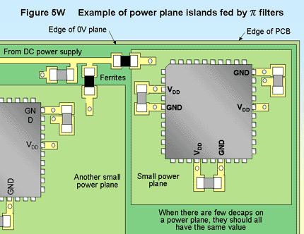
There is little benefit in making the gap between two power plane islands larger than twice the spacing between the layer carrying the power plane islands and the 0V plane layer. If two islands resonate at the same frequency they will suffer very effective coupling across a gap of any size – even from one side of the PCB to another – so either ensure the island’s resonant frequencies are higher than the highest frequency of concern, or else don’t use islands which have the same cavity resonant frequencies. For more on power plane islands, read [22] and [23].
3.8 Damping cavity resonance peaks
IC loads and transmission-line terminations help to dampen 0V/Power plane resonances, so their peak impedances are often not as high as bare-board simulations or tests would suggest. Adding resistors of 1 - 10Ω between two planes adds more losses so also helps damp resonances, but for a 0V/Power plane pair they need to be in series with a capacitor so as not to consume too much DC power. At least one manufacturer offers decaps with an internal series resistance for just this purpose.
There usually only needs to be a few damping resistors spread around a PCB, ideally placed at resonant ‘hot-spots’ where the voltage fluctuations between the 0V and power planes is the highest. The locations of the hot spots may be able to be simulated (see later) or measured – if 0V/Power probing points have been provided at many locations.
In the case of half-wave resonances, such as the first three (lowest frequency) resonances, the hot spots only appear at the power plane corners or along their edges. This observation leads to the technique known as dissipative edge termination, which applies series resistor-capacitor decaps around the perimeter of a power plane [24]. [25] claims that dissipative edge termination is better than the 20-H technique (see below) when the power plane is not ‘shielded’ by extended 0V planes on both sides.
Loading the PCB’s dielectric with particles of ferrite absorber also helps dampen resonant peaks (see section 2.9 of [7]), and may well reduce emissions in other ways. But this is not yet a common method, because the ferrite particles increase the wear on the PCB punching and drilling tools. Maybe when laser-drilled HDI PCB technology (see section 5 of [7], and Part 7 of this series) becomes commonplace, ferrite-loaded substrates will become more attractive.
3.9 The spreading inductance of planes
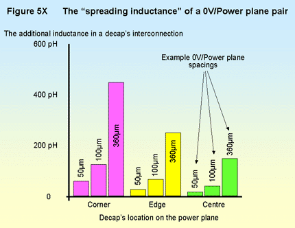
So far in this series planes and 0V/Power plane pairs have been described as if any two points on their surfaces, that were the same distance apart, had the same low impedance between them. But this is not the case – what is called their ‘spreading inductance’ increases the inductance between points placed near to edges, or (worse still) near corners.
This is one of the reasons for the recommendations in earlier parts of this series ([7] and [21]) that planes should extend well beyond all of the devices and traces they are associated with. Figure 5X gives an idea of the scale of this issue. As this figure shows, spreading inductance has less effect when the planes are closer together – another good reason for using very close 0V/Power plane spacing.
3.10 The 20-H rule
Applying the “20-H Rule” means ensuring that the power plane is cut-back from the edge of the 0V plane by a distance equivalent to at least 20 times the spacing between the planes. It is described in Mark Montrose’s books and is often called upon as a means of reducing the edge-fired emissions from a 0V/Power plane structure.
But the 20-H rule only provides significant benefits under certain specific conditions, as described in [25]…
- The rise/fall times of the current fluctuations in the power bus are less than 1ns
- The power plane is on an internal layer of the PCB and has a 0V plane on both sides, each of these 0V planes extending beyond the power plane by a distance that is equivalent to at least 20 times their spacing from the power plane
- The power bus structure is not resonant at any frequencies of concern
- The number of layers in the PCB is 8 or more.
Other techniques described in this series either help the 20-H method to work correctly, or eliminate the need for it.
3.11 Taking advantage of decap series resonances
Some manufacturers put lots of sites for decouplers all over their PCBs (as well as very close to IC power pins). Then, whilst testing emissions, they add decaps with values that have the greatest effect on the lowest frequency at which the emissions are too high. Next, they choose decaps values which suit the 2nd lowest problem frequency – then the 3rd problem frequency, 4th, 5th, etc. They are using the decaps’ SRFs to minimise emissions.
This is a clever way of using the SRF to best effect, but is not generally recommended because it is very sensitive to layout changes, and also sensitive to subtle changes in the capacitors themselves that may not be under the control of the manufacturer.
3.12 Decap walls
The use of power plane islands and π filtering for segregating areas of circuit from each other has already been described (section 3.7). Decap walls is a technique that can be used to reduce the noise that passes from one circuit area to another when they share the same power plane.
Quite simply, the area of circuitry to be protected (or protected from) other circuit areas is completely surrounded by decaps, making a ‘decap wall’ around it. The spacings between the decaps must be small, and their ESLs and interconnect inductances must be low. It is not as effective as using power plane islands, but it may be a useful technique in some situations.
An extension of this technique is to try to reduce emissions from a power plane’s edges by placing a row of decaps around its perimeter. Instead of damping the cavity resonance – as dissipative edge termination tries to do (see section 3.8 above) – this technique tries to create a low impedance around the perimeter so that voltage differences are reduced and the emitted E-field is therefore also reduced.
3.13 Other 0V/Power plane pair techniques to reduce emissions
When a plane pair resonates, its electric field emissions are launched from its perimeter, due to the voltage differences between the two planes at their edges. If all else remains the same – reducing the spacing of the planes reduces the Volts/metre at the plane pair edge and therefore reduces the intensity of the electric fields that are launched [26]. The relationship is linear – halving the plane pair spacing reduces the emissions by 6dB.
As shown elsewhere in this article, reducing the plane pair spacing has a number of other beneficial effects for decoupling for EMC performance – reducing the decaps’ interconnection inductances and increasing the amount of distributed capacitance.
Wrapping the power plane with 0V planes on both sides also helps reduce emissions from a cavity-resonating plane pair [26]. This technique employs the perimeter guard ring technique described in section 2.10 of [7], extending the 0V guard traces as far as possible towards the centre of the PCB. In the limit, the board is completely covered with 0V plane on both sides. Clearly, since there are components mounted on at least one side of the PCB it is impossible to completely shield a PCB without using PCB-mounted shielding cans, as described in section 6 of [7].
Another technique is simply to ensure that the no clock harmonics coincide with the resonant frequencies of the 0V/Power plane cavity (or cavities, when multiple power plane islands are used).
3.14 The buried capacitance technique
The most common PCB buried capacitance technique used to be called Zycon Buried Capacitance (ZBC), which has been used for a several years by a number of computer, cellphone and other manufacturers. Each 0V or power plane in the PCB is converted into a pair of 0V/power planes separated by very thin layer of dielectric. Zycon originally invented the technique, Hadco Corp. then bought them, and Hadco was in turn bought by Sanmina-SCI [27].
Sanmina-SCI offer two products: ZBC1000 and ZBC2000. ZBC1000 uses a ‘core’ consisting of two copper layers separated by 1 thousandth of an inch of FR4, and achieves 900pF/sq. inch (in metric units this corresponds to a thickness of approximately 25µm that achieves 140pF/sq. cm). ZBC2000 uses 2 thousandth of an inch of FR4, and achieves 500pF/sq. inch (in metric units this corresponds to a thickness of approximately 51µm that achieves 77.5pF/sq. cm). It seems that only ZBC2000 is currently used in volume.
Using these products requires no modifications to the PCB layout or its Gerber files by the PCB designer – the bare-board PCB manufacturer simply replaces each 0V or power plane on the PCB with a core of ZBC1000 or 2000, one side being connected to the 0V and the other to the power. Where an original PCB had a single 0V and a single power plane, the result of adding two layers of ZBC2000 is a distributed capacitance of 1000pF/sq. inch (150pF/sq. cm) – considered to be the minimum required to provide good decoupling at frequencies above 500MHz [28].
Figure 5Y shows the stack-up of a 6 layer board with an equally-spaced stack-up and (originally) no embedded 0V/Power plane capacitance. Such PCBs were very common in the 1990’s but when fitted with present day ICs with their faster switching edges they will probably now have poor EMC performance due to their high-impedance power busses. Replacing each plane with a closely-spaced pair of planes, such as ZBC2000, will dramatically reduce their power bus impedance and reduce emissions up to at least 1GHz.

The stack-up shown in Figure 5Y is not ideal for EMC. For example it can be improved by moving each of the two new 0V/Power plane pairs closer to the components on either face of the PCB, to reduce the length of the via holes that carry power bus currents. This issue is explored in more detail in Part 7 of this series.
The use of a 2 thou thick core of FR4 to provide buried capacitance in a PCB is patented, so the only legal way to use this exact technique is for a PCB manufacturer to purchase the ZBC materials from Sanmina-SCI. Although the materials themselves are not very expensive, a license fee has to be paid and this increases the cost. Despite this the net result on the cost of the PCB can be neutral, or even negative, due to the elimination of most/all decaps (apart from ‘bulk’ decaps) and consequent reduction in the area of PCB required for the circuit. The improvement of production yield and reliability in the field, caused by the reduction in the number of components, also helps make a financial case for using ZBC products.
However, it may be possible to avoid infringing the patents when creating your own buried capacitance using a core with a different thickness, or by using 50µm pre-preg layers instead of a 50µm core – but it may be best to check with a patent lawyer first. With such small thicknesses of FR4 the quality of the materials and the accuracy and cleanliness with which they are handled is very important if yields are to be kept high, so if you intend to do follow this route you should probably avoid choosing your PCB manufacturer solely on the basis of the lowest price tendered.
ZBC was originally developed to reduce the number of components on a PCB and thereby reduce size and improve yield and reliability (since there are fewer solder joints to fail). Hadco have said in the past that their users claim ZBC routinely improves their EMC emissions by between 6 and 16dB. But to get the best EMC performance from buried capacitance it should provide enough capacitance to avoid any use of discrete decaps (other than ‘bulk’ capacitance, typically 4.7µF or more) – to avoid the creation of peaks in the power bus impedance due to their parallel resonances.
Unfortunately, 150pF/sq. cm (1000pF/sq. inch) may not be enough to provide good decoupling below 500MHz, depending on the transient current demands of the ICs and other devices. So to able to eliminate all discrete decaps, and hence eliminate their parallel resonances, we may need to use a material with a higher ‘k’ value than FR4.
A great deal of research and development is going on at the moment in the area of buried capacitance, and the alternatives to FR4 that are being developed include...
- EmCap® (Samnina) ceramic powder filled epoxy, k = 36
- Hi-K™ (Dupont) ceramic powder filled polyimide, k = 12
- C-Ply (3M) ceramic powder filled epoxy, k = 21, 5.5nF/sq. inch (850pF/sq. cm)
- FaradFlex™ (Oak-Mitsui Technologies) modified FR4, k = 4, with 12, 16 and 24µm thicknesses, also investigating different materials with higher k that can give up to 40nF/sq. in (6nF/sq. cm).
- Ceramic powder with no binding agent (Fujitsu) k = 400, 300nF/sq. cm [30]
Using a high-k dielectric reduces the propagation velocity for the plane pair, lowering their ‘cavity resonance’ frequencies – not what we really wanted – and causing more resonant peaks to arise in a given frequency range – also not what we really wanted. But closer spacing increases the losses in the cavity, reducing its ‘Q factor’ and reducing the peak amplitudes of the resonances – especially with spacings of 50µm (2 thou) or less. Figure 5Z shows the sort of effects on the power bus impedance of reducing plane pair’s spacing and increasing the k of the dielectric between them.
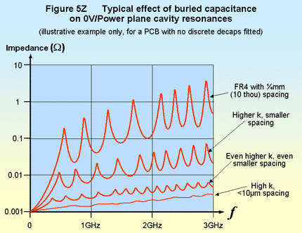
Tests using C-Ply with a thickness of 5µm (0.2 thousandths of an inch) found a Q of 1 in the 0V/Power plane cavity, meaning critical damping – no resonances at all. Since its k was 21, such a thin layer achieved 4nF/sq.cm, giving much higher-performance decoupling than could ever be achieved on a practical PCB using discrete components.
With such thin dielectric (insulating) layers concern naturally arises about breakdown voltages, so it is interesting to note that ZBC1000 is rated for >2500Vdc and is tested at 250Vdc, whilst ZBC2000 is tested at 500Vdc. Tests on a sample PCB made with 10µm thick ‘Faradflex’ found that it withstood 500V. The most likely concerns for voltage withstand with such thin layers concern cleanliness in the PCB manufacturing process and (when using pre-preg layers instead of cores) the accuracy of the alignment of the layers.
It was recently claimed that techniques that achieve 50nF/sq. cm will soon be commercialised, and Fujitsu say that their new ceramic powder technique [29] should cost 40% less than ceramic/polymer composite coatings. So it seems likely that the use of buried capacitance will soon eliminate the use of discrete decouplers (below 4.7µF), using spacings of 25µm (1 thou) or less, and high k. In such PCBs, ‘parallel decoupler’ resonances will only tend to occur below 10MHz, and at such frequencies most sizes of PCBs are very inefficient radiators.
For more on embedded capacitance see [30] and [31].
4. Field solvers for power bus impedance simulations
Part 1 of this series showed, it is very important for commercial success to get to market very quickly, and this implies that the EMC needs to be correct-by-design. But the above shows that decoupling modern ICs is an inexact science, the available components are inadequate (or costly), and the result is that two or more PCB iterations (re-spins) may be required to achieve the desired EMC performance at low cost. It would be wonderful if we could simulate the decoupling of our PCB, from an EMC point of view, so as to get the design right in the virtual world before laying out an actual PCB.
Computer-based simulators using field-solving techniques that simplify Maxwell’s equations have always been able to be used for calculations of power bus impedance, but they have usually required a lot of expertise on the part of their operator, very powerful computers, and their results did not always correspond with real-life behaviour of the simulated PCB assembly.
But developments in EMC simulators are proceeding apace, and user-friendly simulators that run on standard PCs and give reliable answers cannot now be far away. At the IEEE International EMC Symposium in Santa Clara, California, this year a company called EMS-PLUS was advertising what it claimed was an inexpensive simulator for real-world power bus impedances, called EZ-PowerPlane, which it said was easy to use. Another product that claims to help design PCB decoupling is called EMI Stream, from ScanCAD International. Neither of these products claim to calculate the emissions from the simulated PCB at a 10metre distance, but anything that helps achieve good decoupling and the avoidance of high-impedance resonances that are close in the frequency spectrum to the expected problem frequencies, must be of help in reducing time-to-market.
5. EMC-competent QA, change control, cost-reduction
See section 8 of Part 3 [32] for a discussion of this important issue.
6. Compromises
It is easy to write an article like this and simply list all of the relevant good EMC design techniques - but in real-life there are a great many design trade-offs (compromises) to be made, and this is where the circuit and PCB designers really earn their keep.
Designers are often put under cost or time pressure by managers who don’t understand the technical trade-offs, and so don’t understand that their actions could have the opposite effect to that which they intend and actually increase project costs and delays, as well as maybe increasing manufacturing and warranty costs. For more on this topic, please refer to part 1 of this series [6], plus the final section of part 2 [13].
7. References
[1] Keith Armstrong, “Design Techniques for EMC” (in six parts), UK EMC Journal, Jan – Dec 1999
[2] Keith Armstrong, “Design Techniques for EMC” (in six parts), http://www.compliance-club.com/KeithArmstrongPortfolio
[3] M K Armstrong, “PCB Design Techniques for Lowest-Cost EMC Compliance: Part 1”, IEE Electronics and Communication Engineering Journal, Vol. 11 No. 4 August 1999, pages 185-194
[4] M K Armstrong, “PCB Design Techniques for Lowest-Cost EMC Compliance: Part 2”, IEE Electronics and Communication Engineering Journal, Vol. 11 No. 5 October 1999, pages 219-226
[5] “EMC and Electrical Safety Design Manuals”, a set of four volumes edited by Keith Armstrong and published by York EMC Services Ltd., 2002, ISBN 1-902009-07-X, sales@yorkemc.co.uk, phone: +44 (0)1904 434 440.
Volume 1 – What is EMC? ISBN 1-902009-05-3
Volume 2 – EMC Design Techniques – Part 1 ISBN 1-902009-06-1
Volume 3 – EMC Design Techniques – Part 2 ISBN 1-902009-07-X
Volume 4 – Safety of Electrical Equipment ISBN 1-902009-08-8
[6] Keith Armstrong, “Advanced PCB Design and Layout for EMC – Part 1: Saving Time and Cost Overall”, EMC & Compliance Journal, March 2004, pp 31-40, http://www.compliance-club.com/KeithArmstrongPortfolio.
[7] Keith Armstrong, “Advanced PCB Design and Layout for EMC – Part 4:Reference planes for 0V and power”, EMC & Compliance Journal, September 2004, pp 29- 42, http://www.compliance-club.com.
[8] Xilinx, “Powering Xilinx FPGAs”, Application Note ref: XAPP158 (v1.4) Feb 6, 2001, http://www.xilinx.com
[9] Xilinx, “Power Distribution System (PDS) Design: Using Bypass/Decoupling Capacitors”, Application Note ref: XAPP623 (v1.2) June 11, 2003, http://www.xilinx.com
[10] AVX, “Low Inductance Capacitors – Product Brochure”, available from: http://www.avxcorp.com/prodinfo_productdetail.asp?I=35 &ParentID=75 (or Google for ‘interdigitated capacitors’)
[11] For example the on-line inductance calculators kindly provided by the EMC Laboratory at the University of Missouri-Rolla at http://emcsun.ece.umr.edu/new-induct
[12] Theodore M Zeef, Todd H Hubing, Thomas P Van Doren, David Pommerenke, “Analysis of Simple Two-Capacitor Low-Pass Filters”, IEEE Transactions on Electromagnetic Compatibility, Vol. 45, No. 4, Nov 2003, pp 595-601
[13] Keith Armstrong, “Advanced PCB Design and Layout for EMC – Part 2: Segregation and interface suppression ”, EMC & Compliance Journal, May 2004, pp32-42, http://www.compliance-club.com/KeithArmstrongPortfolio.
[14] Douglas G Brooks, “ESR and Bypass Capacitor Self Resonant Behaviour – How to Select Bypass Caps”, UltraCAD Design Inc., available from http://www.ultracad.com.
[15] X2Y Attenuators LLC, “X2Y® Solution for Decoupling Printed Circuit Boards”, application note ref: Note# 1007, V 1.8, 8/26/03, available from www.x2y.com.
[16] Shim, Hwan H, Theodore M Zeeff, Todd H Hubing, “Decoupling Strategies for Printed Circuit Boards without Power Planes”, IEEE International EMC Symposium, 19-23 August 2002, Minneapolis, Minnesota, pages 258-261 in the symposium record.
[17] C N Olsen, T P Van Doren, T H Hubing, J L Drewniak, R E Dubroff, “Improving the High-Frequency Attenuation of Shunt Capacitor Low-Pass Filters”, IEEE International EMC Symposium, Montreal, August 13-17 2001, Symposium Record ISBN 0-7803-6569-0, pp 487-489.
[18] D L Sanders, J P Muccioli, A A Anthony, D J Anthony, “X2Y® Technology used for Decoupling”, IEE seminar, “New EMC Issues in Design: Techniques, Tools and Components”, Qinetiq, Farnborough UK, 28 April 2004, Seminar record: ISBN 0-86341-401-X, pp15-20, sales@iee.org.
[20] Douglas Brooks, Todd Hubing, “Bypass Capacitors – An Interview with Todd Hubing”, UltraCAD Design Inc., available from http://www.ultracad.com. This article also appeared in Printed Circuit Design Magazine, March 1998.
[21] Keith Armstrong, “Advanced PCB Design and Layout for EMC – Part 2: Segregation and Interface Suppression”, EMC & Compliance Journal, May 2004, pp 32- 42, http://www.compliance-club.com/KeithArmstrongPortfolio.
[22] Juan Chen, Todd H Hubing, Thomas P Van Doren, Richard E Dubroff, “Power Bus Isolation Using Power Islands in Printed Circuit Boards”, IEEE Transactions on Electromagnetic Compatibility, Vol. 44, No. 2, May 2002 pp 373-380.
[23] Wei Cui, Juan Fan, Yong Ren, Hao Shi, James L Drewniak, Richard E Dubroff, “DC Power Bus Noise Isolation with Power-Plane Segmentation”, IEEE Transactions on Electromagnetic Compatibility, Vol. 45, No. 2, May 2003 pp 436-442.
[24] Syed A Bokharis, Istavan Novak, “Effect of Dissipative Edge Terminations on the Radiation from Power/Ground Planes”, IEEE International EMC Symposium, 21-25 August 2000, Washington DC, Symposium Record ISBN 0-7803-5677-2, pp 735 – 737.
[25] Mark I Montrose, Liu Enxiao, Er-Ping Li, “Analysis on the Effectiveness of Printed Circuit Board Edge Termination using Discrete Components Instead of Implementing the 20-H Rule”, IEEE International EMC Symposium, 9-13 August 2004, Santa Clara, California USA, Symposium Record ISBN 0-7803-8443-1 (CD-ROM: ISBN 0-7803-8444-X), pp 45-50.
[26] Sergiu Radu, David Hockanson, “An Investigation of PCB Radiated Emissions from Simultaneous Switching Noise”, IEEE International EMC Symposium on EMC, Seattle, August 1999, Symposium Record ISBN 0-7803-5057-X pp 893-898.
[27] Sanmina webpage on PCB fabrication including brochure on Hadco buried capacitance and a licensee list: http://www.sanmina-sci.com/Solutions/pcb_fab.html
[28] Henry W Ott, “Decoupling”, http://www.hottconsultants.com/techtips/decoupling.htm
l
[29] Electronics Weekly, 18 August 2004 page 3 and 1st September 2004 page 7, http://www.electronicsweekly.com
[30] Todd Hubing, M Xu, J Chen, T Van Doren, R DuBroff, “Printed Circuit Board Power Bus Decoupling Using Embedded Capacitance”, EMC Europe 2000, Brugge, 11-15 September 2000, Symposium Record ISBN 90-76019-14-2, pp 639-642.
[31] Minjia Xu, Todd H Hubing, Juan Chen, James L Drewniak, Thomas P Van Doren, Richard E DuBroff, “Mitigating Power Bus Noise with Embedded Capacitance in PCB Designs”, IEEE International EMC Symposium, Montreal, August 13-17 2001, Symposium Record ISBN 0-7803-6569-0, pp 496-500.
[32] Keith Armstrong, “Advanced PCB Design and Layout for EMC – Part 3: PCB-to-chassis bonding”, EMC & Compliance Journal, July 2004, pp 34- 43, http://www.compliance-club.com/KeithArmstrongPortfolio
I would like to reference all of the articles, papers, application notes and textbooks that back-up the techniques described in this series, but the reference list would take longer to write than this series! However, I must mention the papers presented at the annual IEEE International EMC Symposia organised by the IEEE’s EMC Society (http://www.ewh.ieee.org/soc/emcs), especially the dozens of wonderful papers by Todd Hubing and his staff and students at the University of Missouri-Rolla EMC Lab (http://www.emclab.umr.edu), and papers by Bruce Archambeault of IBM and the EMC experts at Sun Microsystems.
Many other contributors to the IEEE EMC Symposia, and other conferences and symposia and private correspondence are far too numerous to be named here, but the following stand out: Tim Williams of Elmac Services, http://www.elmac.co.uk; Mark Montrose of Montrose Compliance Services, http://www.montrosecompliance.com; John Howard, http://www.emcguru.com; Tim Jarvis of RadioCAD, http://www.radiocad.com; Eric Bogatin of Giga-Test Labs, http://www.gigatest.com; and dozens of application notes from National Semiconductor; Rambus Corp.; California Micro Devices; Intel; IBM; Cypress Semiconductor; Xilinx; Sun; Motorola; AVX; X2Y Attenuators; Giga-Test Labs; Ansoft and Flomerics. I apologise to the very many excellent people and companies that I have had to leave out of this list.
Some other useful textbooks are:
[A] Mark I. Montrose, “EMC and the Printed Circuit Board, design, theory, and layout made simple”, IEEE Press, 1999, ISBN 0-7803-4703-X
[B] Mark I. Montrose, “Printed Circuit Board Design Techniques for EMC Compliance, Second Edition”, IEEE Press, 2000, ISBN 0-7803-5376-5
[C] Howard W Johnson and M Graham, “High Speed Digital Design, a Handbook of Black Magic”, Prentice Hall, 1993, ISBN 0-1339-5724-1
[D] Howard W. Johnson, “High Speed Signal Propagation: Advanced Black Magic”, Prentice Hall, 2003, ISBN 0-1308-4408-X
Eur Ing Keith Armstrong C.Eng MIEE MIEEE
Cherry Clough Consultants,
Member of: EMCTLA, EMCUK, EMCIA
keith.armstrong@cherryclough.com