Design Techniques for EMC Part 0 Introduction & Part 1 - Circuit Design and Choice of Components (SECOND PART)
Due to its length we have had to split Part 1 between two issues. This issue contains the second half, Section 1.5 to 1.10. Parts 0 and 1 to 1.4 appear in Issue 62 January 2006.
This is the first in a series of six articles on basic good-practice electromagnetic compatibility (EMC) techniques in electronic design, to be published during 2006. It is intended for designers of electronic modules, products and equipment. To avoid having to write modules/products/equipment throughout - everything that is the result of a design process will be called a ’product’.
This series is an update of the series first published in the UK EMC Journal in 1999 [1], and includes basic good EMC practices relevant for electronic, PCB and mechanical designers in all applications areas (household, commercial, entertainment, industrial, medical and healthcare, automotive, railway, marine, aerospace, military, etc.). Safety risks caused by electromagnetic interference (EMI) are not covered here, see [2] for more on this issue.
These articles deal with the practical issues of what EMC techniques should generally be used and how they should generally be applied. Why they are needed or why they work is not covered, but they are well understood academically and well proven over decades of practice. A good understanding of the basics of EMC is a great benefit in helping to prevent under- or over-engineering, but goes beyond the scope of these articles.
The techniques covered in these six articles will be:
- Circuit design (digital, analogue, switch-mode, communications), and choosing components
- Cables and connectors
- Filters and transient suppressors
- Shielding
- PCB layout (including transmission lines)
- ESD, surge, electromechanical devices, power factor correction, voltage fluctuations, supply dips and dropouts
Many textbooks and articles have been written about all of the above topics, so this magazine article format can do no more than introduce the various issues and point to the most important of the basic good-practice EMC design techniques. References are provided for further study and more in-depth EMC design techniques.
Table of contents for this article
Section 0 and 1.1 to 1.4 are contained in Issue 62, January 2006
0. Introduction to the series
0.1 Cost-effectiveness and time-to-market
0.2 The project EMC lifecycle
1. Circuit design and choice of components for EMC
1.1 Digital: choosing active devices and circuit design
1.1.1 Choosing active devices
1.1.2 Designing digital circuits
1.2 Demodulation and intermodulation
1.2.1 The problem
1.2.2 Designing to prevent demodulation and intermodulation in analogue circuits
1.3 Analogue and data conversion: choosing active devices and circuit design
1.3.1 Choosing active devices
1.3.2 Analogue and data converter circuit design
1.4 Switch-mode power converter design
1.4.1 Circuit topology
1.4.2 Soft-switching
1.4.3 Preventing self-oscillation
1.4.4 Spread spectrum and random modulation techniques
1.4.5 Snubbing
1.4.6 Reducing emissions from heatsinks
1.4.7 Reducing emissions from rectifiers
1.4.8 Reducing emissions due transformer interwinding capacitance
1.4.9 Reducing emissions due to transformer or inductor core conduction
In this Issue:
1.5 Communications circuits
1.5.1 Avoid using metal conductors
1.5.2 Good EMC practices in communications using metal conductors
1.5.3 Opto-coupling and opto-isolation
1.6 Quick and easy in-house tests help choose active devices
1.7 Quick, easy tests on active devices help maintain EMC in serial manufacture
1.8 Choosing passive components
1.8.1 The effects of parasitic R, L and C
1.8.2 Choosing capacitors
1.8.3 Choosing or designing magnetic components
1.8.4 Safety issues
1.9 Second-sourced components
1.10 Some mechanical design and assembly issues
1.11 References
1.12 Acknowledgements
1.5 Communications circuits
The devices used for communications are either digital or analogue, so their selection should take into account the relevant guidelines described earlier.
1.5.1 Avoid using metal conductors
The best communications for EMC purposes are infrared or optical, via free-space (e.g. IRDA) or fibre-optics. Gb/s data rates are available using laser devices, using either free-space or fibre propagation. The transmitters must not have excessive emissions, and the receivers must be immune enough, but these are small devices and their EMC is usually easier to control than that of a long cable. Shielded transmitters and receivers are now readily available.
Most designers automatically assume fibre-optics will be too costly, but plastic fibre-optics at up to 25Mb/s are now being used in large volumes in motor vehicles, driving down the prices of these components (£4.50 for a 25MB/s TX/RX pair in mid-2004). And don’t forget what was said in Part 0 above - the lowest profitable selling price and the one that will maximise the return on investment over the sales life of the product are generally independent of the BOM cost.
It is often practical to take metal-free fibre-optic cables right through the walls of shielded enclosures to PCBs or modules inside, without compromising the enclosure shielding (whereas metal conductors should always be filtered and/or 360° shield bonded at the points where they enter shielded enclosures, see the forthcoming Part 4 of this series, or Part 4 of [1]).
Free-space optical communications may be an appropriate technique, using line-of-sight lasers or more forgiving infra-red. Wireless communications are another good alternative, but their transmitters can sometimes interfere with nearby electronics (depending on transmitter power and proximity) and their receivers can sometimes suffer from interference, so these issues should be taken into account if they are not to create more problems than they solve.
Another reason for using metal-free fibre-optics, free-space optics (e.g. infra-red) or wireless communications is the automatic achievement of galvanic isolation to very high voltages. This often greatly improves product reliability, reduces warranty costs, and avoids the cost, weight and space requirements of filters, surge protection devices, shielding, etc.
Wires and cables may appear at first sight to be the most cost-effective interconnections, but by the time their EMC problems have eventually been solved at the end of a project - the non-metallic alternatives would sometimes have resulted in lower costs overall and shorter timescales.
Wires and cables are usually cost-effective within a product’s fully shielded enclosure, but even then ’intrasystem interference’ problems (one circuit interfering with another inside the product) and the slower propagation velocity in cables can make infra-red, free-space or fibre-optic techniques more attractive.
1.5.2 Good EMC practices in communications using metal conductors
Figures 1M, 1N and 1P outline some examples of bad, better, good and excellent practices in communications, using the example of a 0-10mV transducer connected to a remote circuit by a long cable.

Figure 1M Examples of good and bad practices in signal wiring

Figure 1N Examples of good and bad practices in signal wiring (continued)
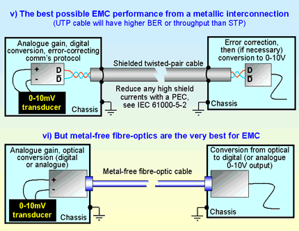
Figure 1P Examples of good and bad practices in signal wiring (continued)
In general, connecting a cable’s shield to a circuit’s 0V is very bad practice for EMC, as is the use of pigtails and grounding cable shields at one end only. Some textbooks still separate cables into low and high frequency types, with different shield-bonding rules for each. But the EM environment is now so polluted with RF up to 2.45GHz (and getting worse all the time) that almost all signals can be expected to suffer from RF noise, so all cables should now be treated as high-frequency types to control EMC.
Figures 1M to 1P show cable shields that are terminated at both ends, with the note that a PEC (Parallel Earth Conductor, according to [19]) should be used if necessary. This topic, and why the resulting ’ground loops’ or ’hum loops’ need not be a problem, up to the very highest level of signal/noise performance, when circuits are designed correctly, is covered in the forthcoming Part 2 of this series, and Part 2 of [1].
For low frequency signals (say, under 10kHz) - the higher the voltage in the communication link the better, for reasons of immunity. But for high frequencies (say, above 1MHz) lower voltages are preferred for reasons of emissions. Most of the highest-speed data communications now use LVDS techniques (Low Voltage Differential Signalling) that have signal levels between 300mV and 1V peak-to-peak.
>em>Communication protocols for improving immunity. Sophisticated error detection and correction protocols can considerably improve the immunity of a communication scheme. Some protocols (such as Ethernet) reduce their data rate the more they are interfered with - so although no bad data gets through and the Bit Error Rate (BER) remains very high, the data throughput rate can fall to zero. Communication protocols that do not reduce their data rate if they suffer from interference are available, and may be preferable in some situations. Do not even imagine that you or your team can design a comm’s protocol that will give good immunity - even after many tens of man-years of development what you have designed will not be as good as protocols that are already commercially available.
Embedded clocks. Where a clock needs to be sent across a communication link, it should be embedded in the data to reduce its emissions. A variety of clock-embedding methods have been well-proven, such as Manchester encoding. Manchester encoding also transfers one bit on each data edge, so halves the data rate in the communications medium for a given ’real’ data rate, which helps reduce emissions too.
Communication protocols for improving emissions. Start and end delimiters, framing and synchronisation bit patterns, token bit patterns, and access control protocols can all have a major influence on how much emitted energy is concentrated into narrow spectral bands during various operational states (high/low traffic, idling, etc.). Appropriate design of the communications protocols should ensure that highly periodic waveforms are always avoided.
Techniques are available (and are used in Gigabit Ethernet) to almost totally randomise data, so that it has no strong spectral components. The emissions are then spreading out across the frequency range instead of being concentrated at specific frequencies.
Matched transmission lines. Transmission line techniques may be essential for good EMC for high-speed analogue or digital signals, depending on the length of their connection and the fastest rise/fall time or highest frequency that will be sent over the cable (see the forthcoming Parts 2 and 5 of this series, or Parts 2 and 5 of [1], and Part 6 of [3] for more detail). It is often not appreciated that the immunity of low-frequency signals may be able to be improved by using matched transmission lines for their interconnections.
The best type of metal cable for EMC purposes usually has a dedicated return conductor twisted with each signal conductor, and a shield that is used only to control interference (not to carry signal return currents). Co-axial cables are generally not preferred for EMC reasons, despite their widespread use by RF engineers and in EMC test laboratories.
Balanced interconnections. Balanced construction twisted-pair or twin-axial cables, or closely-spaced pairs of PCB traces, usually give the best and most cost-effective emissions and immunity performance. For cables, very small differences in twist rate (and even a small difference in the dielectric constants of the pigments used to colour the insulation) can be important for balance at high frequencies. Similar problems affect the balance of differential trace pairs in PCBs (see Part 6 of [3]). Balance is so important that in high-performance circuits a balanced (mirror-image) PCB layout can sometimes be necessary for the devices and their passive components and traces.
It is very important to achieve a good differential balance over the whole frequency range, as this means a good CM rejection ratio (CMRR) and hence improved emissions and immunity. Balanced send/receive ICs are good, but isolation transformers have the benefit of adding galvanic isolation (up to the point where they flash-over) and also extending the CM voltage range well beyond the DC supply rails.
Transformers and balanced send/receive ICs all suffer from degraded balance at RF. They generally require a CM choke to maintain good balance over the whole frequency range of interest, as shown in Figures 1Q and 1R. The CM choke always goes closest to the cable or connector at the boundary of the product.
Figure 1Q Examples of good circuits for high-speed signals or data
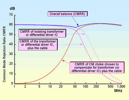
Figure 1R Choose magnetic components to achieve good balance (high CMRR) over the whole frequency range of concern (d.c. to 1GHz in this example)
Figure 1Q shows two examples of circuits that are equally useful for providing good emissions and immunity for digital or analogue communications of any speed or frequency range. These circuits are ideal because they are balanced throughout. Although shielded twisted pair (STP) cable is shown, unshielded twisted pair (UTP) cable could be used but would have worse EMC performance.
Figure 1R shows how the CMRR of the CM choke is tailored to suit the transformer or balanced IC to achieve a good balance (high CMRR) over the whole frequency range of concern.
An alternative type of CM choke is the ’CM transformer’ shown in Figure 1S. An inductor of sufficient value connected between a pair of differential signals has a high impedance to the signals, but if its centre-tap is ’grounded’ it presents a very low impedance to any CM signals superimposed on the differential pair. By centre-tapping one side of the isolation transformer in Figure 1S, it has been made to provide both galvanic isolation and a CM filtering effect. When capacitors are used in series with the centre-tap, their resonances (see later) can affect the performance of the CM transformer.
Where a balanced send or receive IC is used, the ’IC side’ winding of the transformer could be centre-tapped instead of the ’cable side’, and the centre tap connected to the 0V (via a capacitor if necessary for biasing reasons) to provide CM rejection. Maybe improved performance could be had by centre-tapping both windings and RF bonding them both to their respective references.
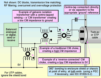
Figure 1S ’CM transformers’ and ’reverse-connected’ CM chokes
Another alternative to the ’traditional’ CM choke is to connect one in reverse [20], as shown in Figure 1S. This creates a low impedance to CM noise, like the CM transformer it closely resembles. The low CM impedance of the CM transformer and reverse-connected CM choke techniques contrasts with the high CM impedance of the more traditional CM choke, so combining these CM suppression techniques in one circuit, as shown in Figure 1S, can provide very powerful CM suppression. Some manufacturers provide magnetic components for serial datacommunications that combine one or more CM chokes, isolation transformers and CM transformers in a small module.
Where co-axial cables are used instead of twisted-pairs or twin-ax, EMC and signal integrity will suffer because the cable isn’t a balanced type, and also because the shield carries the signal return current as well as the noise currents due to RF fields and potential difference between the products at both ends. The techniques shown in Figure 1T will help to achieve the best possible performance from coaxial cables used. Circuits without isolation transformers will generally suffer from poorer immunity at lower frequencies.
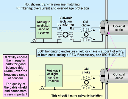
Figure 1T Co-axial cable communications circuits
Low performance datacommunications often use multi-conductor cables to save cost, as shown by Figure 1U, an example of an RS232 application. The EMC of these will generally benefit from the use of CM chokes - where a conductor has N cores, it is generally best to connect it to the electronics at each end via a CM choke with N windings.

Figure 1U Example of low-rate datacommunications (RS232 in this case)
1.5.3 Opto-coupling and opto-isolation
Opto isolation/coupling techniques using packaged devices are commonly used, especially for digital signals, but the input-output stray capacitance associated with typical devices is a little under 1pF - a high enough value to create a low impedance at frequencies above 100MHz to interact with the circuit impedances and destroy the balance of the signals in the cable, or to interfere with the circuits on the circuit side of the opto device.
Where signals with very short rise/fall times are to be communicated, it may be necessary to employ a suitable CM choke to maintain the balance at high frequencies, as shown by Figure 1V.
But where opto-couplers are used for slow data signals they often use unbalanced coaxial cables, or multi-conductor cables with a single wire for each signal (and a common return). In these cases a single soft ferrite bead in series with each signal line to an opto-coupler may be all that is needed to prevent RF interference.
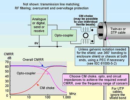
Figure 1V Example of very high-data rate optocoupling
Opto devices are available with very low input-to-output stray capacitance, achieved by the use of a short light-pipe inside. These are usually intended for high-voltage use. There are also opto devices available with internal shields, usually intended for use in feedback loops in switch-mode power converters and designed to withstand very high levels of noise at frequencies up to 1MHz or so. Although these devices will provide better EMC performance, most of them are not intended for use with very high data rates, very short rise/fall times, or very high frequency analogue signals.
Analogue signals can now benefit from opto-isolation with 0.1% linearity, using devices such as the IL300. This can save having to use voltage-frequency (and frequency-voltage) converters in many opto-coupled applications, or replace bulky transformers.
Because of the common drawing practice of not showing power rails in full on schematics, it sometimes happens that both sides of an opto-isolator are accidentally powered from the same DC power rails, seriously compromising the isolation achieved and the EMC performance. The RF performance of opto-isolators can only be as good as the RF isolation between the power supplies associated with each side of an opto device.
1.6 Quick and easy in-house tests help choose active devices
It is usually the case that a device’s real-life EMC performance is unknown, despite the claims made by its suppliers. There are easy and quick EMC testing methods that can be applied in-house, on simple functional circuits that at least run the clocks and preferably perform signal or data I/O operations at full speed too. Some suppliers offer evaluation boards that can be used for these tests.
Testing for emissions can easily be done in a few minutes on a standard test bench with a close-field magnetic loop probe connected to a spectrum analyser or wideband oscilloscope (see Parts 1 and 2 of [7]). Some devices will very quickly be seen to be much quieter than others.
Testing for immunity can use the same probe connected to the output of a signal generator (either continuous RF or transient) - but if it is a proprietary probe (and not just a shorted turn of wire) first check that its power handling is adequate. Refer to Parts 3, 4 and 5 of [7] for appropriate techniques.
Close-field probes need to be held almost touching the devices or PCBs being probed. To locate the "hottest spots" and optimise probe orientation they should first be scanned in a horizontal and vertical matrix over the whole area (holding the probe in different orientations at 90° to each other for each direction), then concentrating on the areas with the strongest signals.
Some digital ICs radiate emissions strongly from their own bodies, rather than conduct them through their pins. They may benefit from being shielded with their own little metal box soldered to the PCB’s 0V plane. Shielding at PCB level is very low-cost, and is covered in the forthcoming Parts 4 and 5 of this series, Parts 4 and 5 of [1], and in more detail in Part 2 of [3].
A very few manufacturers offer a few of their IC products with guaranteed EMC emissions and immunity specifications, usually measured in bench-top testers. These are more likely to be complex ICs for use in cellphones and similar products.
1.7 Quick, easy tests on active devices help maintain EMC in serial manufacture
Batches of ICs from the same manufacturers can have different EMC performances, due to the use of silicon processes with smaller features. Device manufacturers are constantly reducing the silicon feature sizes of their devices to fit more of them on a wafer and reduce their costs. This is especially true for digital ICs, where they call it ’mask-shrinking’ or ’die-shrinking’.
Larger purchasers can arrange to get advance warnings of mask-shrinks so they can buy enough of the ’old’ ICs to keep them in production while they find out how to deal with the changed EMC from the new mask-shrunk IC. Even with 6 months warning, the EMC consequences are known to have cost at least one large manufacturer tens of millions of US dollars.
It is possible to perform simple checks of IC EMC performance when active devices are first delivered to the ’goods-receiving’ department, to see whether they have different EMC performance, for whatever reason. This helps discover problems early on, and reduces financial risks. Alternatively, or in addition, sample-based EMC testing in serial manufacture helps avoid shipping non-compliant or unreliable products. Some EMC test methods suitable for use in goods-receiving and manufacturing test are described in [7].
1.8 Choosing passive components
1.8.1 The effects of parasitic R, L and C
All passive components suffer from ’parasitic’ resistance, inductance and capacitance (often called stray R, L and C). At a high enough frequency these will dominate the impedance of the components and completely alter their circuit behaviour. Helpful manufacturers of quality components publish data on strays, the most useful being their impedance versus frequency over the range of frequencies of concern. (Never choose a ferrite suppressor without such a curve.)
For example, at high frequencies a leaded film resistor can act either as a capacitor (due to its shunt C of around 0.2pF) or as an inductor (due to the L of its leads plus its spiralled tolerancing cut). Wire-wound resistors above a few kHz have an impedance which is not what was marked on their box (even ’low-inductance’ types), whereas leaded film resistors under 1kΩ usually remain resistive up to a few hundred MHz. See Figure 1W for a simplified analysis of typical surface mounted resistors.

Figure 1W Example of a first-order equivalent circuit for a surface mounted resistor
Capacitors self-resonate due to their internal interconnect inductance, and at higher frequencies their impedances are mostly inductive, see Figure 1X for a simplified analysis of a typical multilayer ceramic surface mounted capacitor.
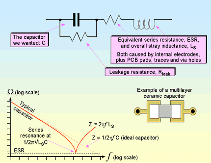
Figure 1X Example of a first-order equivalent circuit for a surface mounted capacitor
Inductors self-resonate due to their internal and interconnect inductance, and their interwinding capacitance. See Figure 1Y for a simplified analysis of a typical surface mounted inductor (note: this is not a soft-ferrite RF suppressor type).
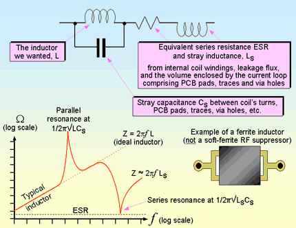
Figure 1Y Example of a first-order equivalent circuit for a surface mounted inductor
Where leaded components are important for good EMC, their lead lengths should be well-controlled in serial manufacture (just adding 5mm of lead length to a PCB-mounted component can completely ruin its RF and EMC characteristics). Surface mounted components are preferred for EMC because they cannot suffer from lead-length variations, plus they are smaller so their strays are generally lower, so they generally maintain their nominal values up to a much higher frequency. For example, SMD ’chip’ resistors under 1kΩ (but not MELF types) are usually resistive to at least 1GHz.
All components have a limited power handling capacity (both transient and continuous dissipation ratings), a limited dV/dt capacity (e.g. tantalums go short-circuit if their dV/dt limit is exceeded), a limited dI/dt capability, etc. SMD parts, being smaller, generally have lower wattage ratings than leaded parts.
The parasitic Rs, Ls and Cs in passive components makes filter design much more complicated than the circuits in textbooks or on computer simulators might suggest. Where a passive component is to be used with high frequencies (e.g. to divert interfering currents up to 1GHz to a 0V plane) it is vital to understand all about its strays and to do a few simple sums to work out their effects.
The use of components with unknown parasitics for high-speed signals and/or EMC purposes makes it more likely that the number of product design iterations will be high and time-to-market delayed.
1.8.2 Choosing capacitors
Ceramic dielectrics usually give the best high frequency performance, so SMD ceramics are often excellent. Some ceramic dielectrics have strong temperature or voltage coefficients, but COG or NPO dielectric materials have no significant temperature, frequency, or voltage coefficients, so make very stable and rugged high-quality high-frequency or pulse-handling capacitors.
There are many other issues relating to selection of capacitors, including RF impedance, pulse-handling capability, equivalent series resistance (ESR), equivalent series inductance (ESL), tolerance, ageing, etc. Very low ESR is a very important EMC requirement for the bulk storage capacitors in switch-mode power converters.
Electrolytic capacitors are ineffectual at frequencies above a few MHz, so often need to be paralleled with ceramic capacitors. Replacing electrolytics completely with multilayer ceramic capacitors (MLCC) is often a good thing for EMC and long-term reliability - it seems that the lower ESRs of the MLCCs (now available with up to 100µF in small case sizes at low DC voltage) means that an electrolytic can be replaced by an MLCC that has between one-half and one-fifth of its value, depending on the application.
1.8.3 Choosing or designing magnetic components
The magnetic circuits of inductors and transformers should be closed to reduce magnetic field emissions, for example by using toroids or other types of gapless cores, for immunity as well as for emissions. Rod-cored chokes or inductors must be used with great care, if they cannot be avoided altogether. Inductors wound on ferrite rods make good RF antennas (and are used for that purpose in AM radios) - not what we need for good EMC. Toroidal mains transformers in linear power supplies are gapless, and can have lower ’hum’ fields than standard rectangular core types.
Energy storage inductors in switch-mode converters must have an air gap, but iron powder toroidal types effectively store their energy in the microscopic air gaps between the iron particles, distributed around the body of the toroid, so emit lower fields than gapped cores.
If air gaps have to be used, an overall shorted turn may be needed to reduce the leakage fields. It is important to understand that ’overall’ means that the turn is around the entire body of the component, so that it is only a shorted turn for the leakage fields. Shorting turns are used to reduce emissions from switch-mode power converter magnetics, and also to improve the immunity of microphone and other sensitive transformers.
The current flowing in an inductor directly affects its inductance value, so it is important to know what this coefficient is to design circuits (e.g. filters) correctly. High temperatures also have an effect on inductance, as temperatures rise above about 50°C inductance falls more and more quickly until the Curie point is reached, at which temperature the material loses all its inductance (cooling below the Curie point restores the inductance).
Other issues to consider in the choice of magnetic components include saturation (when inductance drops to zero) and the possibility of overheating due to dissipation in both core and the windings. Ferrite cores are not insulators, so in some cases may need to be coated with a tough insulator.
1.8.4 Safety issues
Some active devices and passive components will need to be rated for safety, especially all those connected to hazardous voltages such as the AC mains supply. In such cases it is best to only use parts which have been approved to the correct safety standard(s) at the correct ratings by an accredited third-party laboratory and allowed to carry their distinguishing mark (e.g. VDE, UL, CSA, SEMKO, DEMKO, NEMCO, BSI, TUV, etc. But you can’t rely on the presence of an agency mark on the component, or on its data sheet - they could be forgeries.
Due diligence in safety requires getting a copy of the safety approval certificates and/or test reports for the components concerned, and then...
- checking with the issuing laboratories that they are not forgeries,
- checking that their tested ratings are what you need for your design,
- checking that they fully comply with all the parts of all the necessary safety standards for your design.
A procedure should also be in place to check that components delivered for assembly into a manufacturer’s products are not counterfeit. About 5% of world trade is estimated to be counterfeit, including such safety-related components such as mains cords, fuses and circuit-breakers. This is public knowledge, so if a counterfeit component caused a safety incident the manufacturer might be held fully liable under the Low Voltage Directive, General Product Safety Directive, or Product Liability Directive for not taking the necessary precautions.
1.9 Second-sourced components
ICs, transistors and passive components from different manufacturers can have very different EMC performances even if they have the same part number and data sheet specifications. Costly test laboratory EMC testing on products fitted with second-source components may not be required on the second-source devices, however, where appropriate quick and easy in-house tests (see [7]) show no significant differences for emissions or immunity. If no EMC testing is to be done on the second-sourced components it will be best to use single sourced devices.
1.10 Some mechanical design and assembly issues
- Place noisy or sensitive devices as far from conductors as possible. Noisy devices include all crystal oscillators, ICs and transistors that operate at high clock speeds. Conductors include PCB traces, connectors, wires, cables, structural elements (e.g. brackets), etc. When a product is finally assembled, flexible wires, cables and other conductors inside its enclosure can often lie in a wide variety of positions - it is very important to ensure that no such wires or cables might lie on top of (or nearby) any high-speed digital or data conversion, or sensitive analogue devices.
- ’Ground’ heatsinks. A heatsink is a conductor, and clearly must have at least a part of itself in intimate proximity to the device it is cooling. But heatsinks can suffer from coupled signals from inside an IC just like any other conductor. The usual technique is to isolate the heatsink from the IC with a thermal conductor (the thicker the better as long as thermal dissipation targets are met), then ’ground’ the heatsink to the PCBs 0V plane local to the device being cooled with many very short connections (the mechanical fixings can often be used). To reduce radiation at 100MHz and above, a heatsink needs evenly distributed 0V connections all around its perimeter - better still, a continuous peripheral connection via a conductive gasket. See Part 8 of [3] for more on this.
Heatsinks for off-line switchers were discussed earlier - be sure to deal fully with all possible safety issues.
- Avoid sockets. IC sockets are very bad for EMC, and directly soldered surface-mounted ICs (or chip and wire, or similar direct chip termination techniques) are preferred. Where motherboards are fitted with ZIF sockets and spring-mounted heatsinks to allow easy processor upgrading, EMC performance will not be the best and the additional filtering and shielding performance required will increase costs. It will help to choose surface-mounted ZIF sockets with the shortest lengths of internal metalwork for their contacts.
- Use smaller, lower profile IC packages. These can give improved emissions and immunity on PCBs fitted with 0V planes (see the forthcoming Part 5 of this series, Part 5 of [1], or Part 4 of [3]). Very small devices (e.g. chip-scale packaging, flip chip, micro-BGA) can be used to produce very low-cost PCBs with very good EMC if advanced PCB design and manufacturing techniques [3] are used.
1.11 References
[1] Keith Armstrong, "Design Techniques for EMC", UK EMC Journal, a 6-part series published bimonthly February - December 1999. An improved version of this original series is available via the "Publications & Downloads" page at http://www.cherryclough.com.
[2] The Institution of Electrical Engineers (IEE), Professional Network on Functional Safety, "EMC and Functional Safety Resource List", via the "Publications & Downloads" page at http://www.cherryclough.com.
[3] Keith Armstrong, "Advanced PCB Design and Layout Techniques for EMC", an 8-part series published in the EMC & Compliance Journal, March 2004 - November 2005. An improved version of this series is available via the "Publications & Downloads" page at http://www.cherryclough.com.
[4] Keith Armstrong, "Assessing an EM Environment", includes informative tables, an example of an initial questionnaire, guidance and useful references, available via the "Publications & Downloads" page at http://www.cherryclough.com.
[5] Keith Armstrong, "EMC for Systems and Installations", a 6-part series published in the EMC+Compliance Journal, January-December 2000, also available via the "Publications & Downloads" page at http://www.cherryclough.com.
[6] Tim Williams and Keith Armstrong, "EMC for Systems and Installations", Newnes 2000, ISBN 0 7506 4167 3, www.newnespress.com, RS Components Part No. 377-6463.
[7] Tim Williams and Keith Armstrong, "EMC Testing", a 7-part series published in the February 2001 - March 2002, available via the "Publications & Downloads" page at http://www.cherryclough.com.
[8] A series of 17 booklets on EMC testing using the basic EN or IEC test methods, including details of what causes the EM phenomena and how they cause interference, written by Keith Armstrong and published by REO (UK) Ltd, available via the "Publications & Downloads" page at http://www.cherryclough.com.
[9] Three articles by John R Barnes: "Designing Electronic Equipment for ESD Immunity", Printed Circuit Design, vol. 18 no. 7, July 2001, pp. 18-26, http://www.dbicorporation.com/esd-art1.htm; "Designing Electronic Equipment for ESD Immunity Part II", Printed Circuit Design, Nov. 2001, http://www.dbicorporation.com/esd-art2.htm; "Designing Electronic Systems for ESD Immunity",
Conformity, Vol. 8 No. 1, Feb. 2003, pp. 18-27, http://www.conformity.com/0302designing.pdf. The software techniques described here are useful for all EMC immunity issues, not just ESD.
[10]John R Barnes, "Robust Electronic Design Reference Book, Volume I", Kluwer Academic Publishers, 2004, ISBN: 1-4020-7737-8
[11]Tim Williams, EMC for Product Designers 3rd edition, Newnes 2001, ISBN: 0-7506-4930-5, www.newnespress.com.
[12]Steve Sheafor of X-EMI Inc., "Next Generation EMI Reduction techniques", Interference Technology’s EMC Directory & Design Guide 2005, pp 100-108, http://www.InterferenceTechnology.com.
[13]Nick Holland and Mike Score, "Eliminating the Audible Buzz in GSM Phones", Microwave Engineering, December 2005/January 2006, pp23-24, http://www.mwee.com.
[14]Analog Devices Application Notes: visit http://www.analog.com, click on ’Design Center’, then click on ’Application Notes’, especially recommended are: AN 202, AN 214, AN244, AN 257, AN 345, AN 347 and AN 348.
[15]Y Touzani, P Le Bars, J P Toumazet, A Laurent, "The Effects of RPWM on the Conducted Electromagnetic Emissions in Bidirectional Three-Phase Unity Power Factor Boost-Buck Converter", EMC Europe Symposium 2004, Eindhoven, The Netherlands, Sep 6-10 2004, pp 656-661.
[16]M Melit, N Boudjerda, B Nekhoul, L El khamlichi Drissi, K Kerroun, "Random Modulations for Reducing Conducted Perturbations in DC/DC Converters", EMC Europe Symposium 2004, Eindhoven, The Netherlands, Sep 6-10 2004, pp 650-655.
[17]Carli Giampaolo, "Saturable Bead Improves Reverse Recovery", EDN magazine, 3rd February 1997, pages 92-94, http://www.edn.com/archives/1997/020397/03DI_03.htm.
[18]M Martijak, L Filipic, "Decreasing Conducted Emissions with Transformer Design", EMC Europe Symposium 2004, Eindhoven, The Netherlands, Sep 6-10 2004, pp 639-644.
[19]IEC 61000-5-2:1997 "Electromagnetic Compatibility (EMC) - Part 5: Installation and Mitigation Guidelines - Section 2: Earthing and Cabling", http://www.iec.ch.
[20]H Suenaga, O Shibata and Y Saito, "Termination with a Reverse-Connected Common-Mode Choke (T-ReCC) for a Differential Line", IEEE 2005 International Symposium on EMC, Chicago, August 8-12, ISBN: 0-7803-9380-5, pp 175-178.
1.12 Acknowledgements/h3>
I am very grateful to the following people for suggesting a number of corrections, modifications and additions to the first series published in 1999: Feng Chen, Kevin Ellis, Neil Helsby, Alan Keenan, Mike Langrish, Tom Liszka, Tom Sato, and John Woodgate.
Eur Ing Keith Armstrong C.Eng MIEE MIEEE
Partner, Cherry Clough Consultants
www.cherryclough.com, Member EMCIA
keith.armstrong@cherryclough.com
Tel: +44 (0)1457 871605 Fax: +44 (0)1457 820145