Design Techniques for EMC Part 4 - Shielding (Screening)(part 1)
This is the fourth in a series of six articles on basic good-practice electromagnetic compatibility (EMC) techniques in electronic design, to be published during 2006-7. It is intended for designers of electronic modules, products and equipment, but to avoid having to write modules/products/equipment throughout - everything that is sold as the result of a design process will be called a ’product’ here.
This series is an update of the series first published in the UK EMC Journal in 1999 [1], and includes basic good EMC practices relevant for electronic, printed-circuit-board (PCB) and mechanical designers in all applications areas (household, commercial, entertainment, industrial, medical and healthcare, automotive, railway, marine, aerospace, military, etc.). Safety risks caused by electromagnetic interference (EMI) are not covered here; see [2] for more on this issue.
These articles deal with the practical issues of what EMC techniques should generally be used and how they should generally be applied. Why they are needed or why they work is not covered (or, at least, not covered in any theoretical depth) - but they are well understood academically and well proven over decades of practice. A good understanding of the basics of EMC is a great benefit in helping to prevent under- or over-engineering, but goes beyond the scope of these articles.
The techniques covered in these six articles will be:
- Circuit design (digital, analogue, switch-mode, communications), and choosing components
- Cables and connectors
- Filtering and suppressing transients
- Shielding (screening)
- PCB layout (including transmission lines)
- ESD, surge, electromechanical devices, power factor correction, voltage fluctuations, supply dips and dropouts
Many textbooks and articles have been written about all of the above topics, so this magazine article format can do no more than introduce the various issues and point to the most important of the basic good-practice EMC design techniques. References are provided for further study and more in-depth EMC design techniques.
Table of contents for this article
4. Part 4 - Shielding (screening)
4.1 Introduction
4.2 Shielding with metal plates
4.3 Volumetric shielding of products
4.3.1 Nested shielding and cost-of-manufacture
4.3.2 General concepts in volumetric shielding
4.3.3 Skin effect and absorption
4.3.4 Very low frequency shielding
4.3.5 SE is compromised by leakage from apertures
4.3.6 The resonant/antenna behaviour of a single aperture in the far field
4.3.7 Multiple apertures in the far field
4.3.8 Cavity resonances and aperture leakage
4.3.9 Near-field leakages through apertures
4.3.10 Designing to reduce aperture leakages
4.3.11 Waveguide-below-cutoff techniques
The following will appear in the next issue
4.3.12 Shielding of displays (and the like)
4.3.13 Shielding membrane switch panels
4.3.14 Shielding ventilation apertures
4.3.15 Shielding rotating metal shafts that penetrate an enclosure
4.3.16 Combining heatsinking with enclosure shielding
4.3.17 Preventing shield degradation from conductor penetrations 4.3.18 The synergy of shielding and filtering
4.3.19 Installation of shielded enclosures
4.4 Shielding at PCB level
4.4.1 Reasons for shielding at PCB level
4.4.2 Overview of techniques for PCB level shielding
4.4.3 Types of PCB shielding can
4.4.4 Methods for bonding shielding cans to PCB planes
4.4.5 Suitable materials for PCB shielding cans
4.4.6 Apertures in PCB shielding cans
4.4.7 Waveguide below cut-off methods in PCB- level shielding
4.4.8 Cavity resonances in PCB shielding cans
4.4.9 Conductors entering/exiting PCB shielding cans
4.4.10 Combining filtering with shielding at PCB level
4.4.11 Combing heatsinking with shielding at PCB level
4.5 Estimating shielding effectiveness with PC-based simulators
4.6 EMC gaskets
4.6.1 Mechanical design techniques for gaskets
4.6.2 Gasket clamping
4.7 Materials useful for shielding
4.7.1 Metals and their surface finishes
4.7.2 The problems of polymer passivation
4.7.3 Papers and fabrics
4.7.4 Paints and lacquers
4.7.5 Painted or plated plastics
4.7.6 Shielding with volume-conductive plastics
4.7.7 Alternatives to shielding plastic enclosures
4.7.8 Environmental considerations
4.7.9 Preventing corrosion
4.8 References
4.9 Acknowledgements
4. Part 4 - Shielding (screening)
4.1 Introduction
Shielding is used to attenuate unwanted frequencies travelling through the air, or through whatever the product is immersed within (e.g. vacuum, oil, etc.) - and shields are characterised by attenuation versus frequency curves. In many ways, electromagnetic (EM) shields are the radiated-wave equivalents of EM filters, which attenuate conducted EM waves (see Part 3 of this series [3]). As will be shown later, and was discussed in section 3.3.3 of [3], shielding and filtering generally have to be used together, in order for either one to provide the EMC benefits required.
This article uses the word ’shield’ instead of ’screen’, because screen has some other common uses in electronics (e.g. display screen). Cable shielding was dealt with in section 2.6 of [4], so this article is concerned with other types of shields. Note that for cable shielding to function well, especially at frequencies above 100MHz, the equipment connected to either end of the shielded cable also needs to be shielded, with its shield bonded 360ø to the cable shield.
Figure 4A shows the radiated EM spectrum up to 2.5GHz, and some of its commonplace civilian uses. The spectrum above 2.5GHz is being developed very quickly, as low-cost semiconductors that can operate at such frequencies are developed.

Figure 4A The radiated spectrum and its uses (only up to 2.5GHz shown)
Figure 4B shows the typical EM spectra of the noises radiated by some commonplace electronic devices, and an example of the radiated noise caused by sparking at an electrical contact. It is clear that to be able to use the radiated spectrum for broadcasting, communications, etc., we must protect it from electronic and electrical noise.

Figure 4B The spectra of noises made by electrical/electronic devices (only up to 2.5GHz shown)
For the above reasons, shielding is a technique that has been used for many years, and Figure 4C shows part of a method for testing shielding effectiveness (SE) dating from 1882 (kindly provided by Anton Kohling of Siemens EMC Test Laboratory in Erlangen).

Figure 4C Shielding Effectiveness testing in 1882
Inadequately designed shielding can make a product’s emissions or immunity worse than it was without the shield. One cannot, in general, simply select a shielded enclosure from a supplier’s catalogue and expect that no more work will be required - there are numerous design and assembly techniques that need to be taken into account if the purchased enclosure is to provide the shielding performance required. It is very easy to completely negate a shielded enclosure’s performance by not paying sufficient attention to the issues discussed in this article.
Many textbooks and learned papers have been written on shielding and Chapter 34 of [5] includes a very comprehensive list of them. There are also now a number of simulators that run on PCs and can be used to simulate the effects of shields. This article will not go into wave equations and that sort of detail - instead it will describe the things that need to be taken into account so that shielding stands a good chance of performing as required, and to avoid unpleasant and/or costly experiences.
Shielding design or selection is not a ’black art’, but nevertheless it is difficult to predict exactly what performance a given shield construction will achieve when installed in a product, especially at frequencies above 100MHz, so it is often necessary to experiment with different options to find the most cost-effective. Planning and designing for such flexibility from the start of a project is very worthwhile, and an example of what John R Barnes [5] calls "wiggle room" and I call "anti-Murphy design". My approach is based upon the well-known Murphy’s Law - I find that designers who try to anticipate the surprises that Murphy might have in store for them reach their design targets and timescales more reliably, and the resulting products have a lower overall cost of manufacture because they have not had to have shields (or more complex shields than were hoped for) squeezed in somehow at the end of a project when compliance tests were failed.
Shields are always fitted at a boundary between two zones, one of which needs to be protected from the EM fields present in the other. This article generally considers shields that are fitted at the boundary between a product and its external EM environment - shielded overall product enclosures. Shields can also be used inside a product, for example between a switch-mode power supply and a sensitive analogue circuit, and their design will employ most, if not all, of the same design techniques.
4.2 Shielding with metal plates
The ’image plane’ effect means that large metal surfaces can provide useful amounts of shielding for components and conductors that are placed close enough to them - for example, by using low-profile PCB components with an overall PCB plane, or by locating all PCBs and routing all cables close to a large metal chassis, frame, or enclosure. To be effective, the metal surface needs to have much larger dimensions than the components or conductors, and the spacing from the metal surface needs to be less than one-tenth of a wavelength (λ/10) at the highest frequency for which any shielding effectiveness is required. Closer spacings are better. When spacings are less than about λ/6, SE can become negative (i.e. provide gain), possibly worsening emissions or immunity compared with doing nothing.
Electrical bonding between the metal surface and the components or conductors helps to control and return common-mode (CM) currents, also helping to improve SE. For this to be effective, the electrical bonds must have a very low impedance (say <1Ω) at the highest frequency for which improvement is required. Note that impedance does not mean resistance - at radio frequencies (RF) it is usually the inductive reactance (2πfL) that is most significant, and <1Ω at, say, 300MHz, implies an inductance of about 530pH. Ordinary thin wire has an inductance of about 1nH per millimetre length.
This technique might provide sufficient SE to eliminate the need for a shielded enclosure, or at least to reduce its SE specifications and hence its cost. Because EMC engineers work in dB, it is easy to overlook the importance of a small improvement, say 3dB. 3dB does not sound like worth bothering with, but it represents a 50% improvement in SE performance, and at frequencies above 300MHz quite possibly a 50% (or more) increase in the overall cost of manufacture of a shielded enclosure. So it is cost-effective to take every chance to improve SE by a few dB, rather than leave all the shielding to the overall enclosure.
4.3 Volumetric shielding of products
Most shields will need to be volumetric - surrounding the product to be shielded in all three dimensions - such as a six-faced rectangular box. This section discusses the design and assembly of volumetric shields applied to an entire product.
A complete volumetric shield is often known as a ’Faraday Cage’, although this can give the impression that a box full of holes (like Mr Faraday’s original version) is acceptable, which it generally is not.
As mentioned earlier, shields can also be used inside products, to protect one zone from EM fields generated in another. The same design techniques apply to these shields as for overall enclosure shields.
4.3.1 Nested shielding and cost-of-manufacture
There is a cost hierarchy to shielding which makes it important to take shielding into account very early in the design process. Shields may be fitted around:
- Individual ICs or small areas on a PCB relative cost 1
- Whole PCBs relative cost 10
- Sub-assemblies and modules relative cost 15
- Complete products relative cost 100
- Assemblies (e.g. industrial control cubicles) relative cost 1,000
- Rooms relative cost 10,000
- Buildings relative cost 100,000
These relative costs are only very approximate, and are only concerned with overall cost-of-manufacture. They do not cover the costs and delays of adding unanticipated shielding late in a project, which can be very much greater.
To save cost, devices should be chosen and circuits designed as described in Part 1 of this series [6] to reduce their need for shielding; then their PCBs should be designed so that shielding can be applied to them (see later); then any modules and sub-assemblies designed so that shielding can be applied to them. Finally, the overall enclosure should be designed so that shielding can be applied.
Shielding always adds cost and weight, but the above approach will generally achieve the lowest overall costs-of manufacture whilst also considerably reducing delays and re-engineering costs if improvements in SE are found to be required late in a project, when design freedom is circumscribed and even simple changes can be very costly (see Part 0 of [6]). It can be very difficult indeed to retrofit shielding to a metal or plastic enclosure that was not originally designed to be able to be shielded, as later sections will make clear.
’Nested’ low-cost shielding, as shown by Figure 4D, is usually not only more cost-effective than relying on a single overall enclosure shield - it is also more reliable. For example: if 60dB of shielding is required at 900MHz and is achieved solely by a shielded overall enclosure, a small defect in the enclosure or its assembly could easily reduce the SE to 20dB or less. But if three levels of lower-cost shielding are employed as shown in Figure 4D, each one giving 30dB at 900MHz, the overall cost of manufacture could be less, and the outer enclosure could suffer defects or damage, or foreseeable misuse (e.g. removing a cover) without the overall SE dropping below the required 60dB.
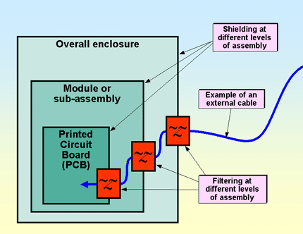
Figure 4D Example of ’nested’ shielding and filtering
The requirements for cost-effective manufacture should always be taken into account during design. A shield design suitable for product hand-made in small volumes might not be at all appropriate for products manufactured on automated production lines in tens of thousands. The cost pressures on high-volume manufacture generally mean that shielding on the PCB is preferred to enclosure shielding. Indeed, as will be shown later, above 1GHz it can be very difficult/costly to rely entirely on enclosure shielding, and PCB-level shielding is almost essential.
4.3.2 General concepts in volumetric shielding
A shield puts an impedance discontinuity in the path of a propagating radiated EM wave, reflecting it and/or absorbing it. This is conceptually very similar to the way in which filters work - they put an impedance discontinuity in the path of an unwanted conducted EM wave. The greater the impedance ratio between wave and shield, the greater the SE achieved.
Figure 4E shows the overall operation of a shield. Depending on its wave impedance, a proportion of the incident wave is reflected at the first ’high-low’ impedance discontinuity (the facing surface of the conductor), and the remainder carries on inside the material as a transmitted wave, being absorbed by being turned into heat by the resistivity of the material. When the transmitted wave hits the ’low-high’ impedance discontinuity at the other surface of the conductor, a proportion is again reflected and stays inside the conductor, while the remainder exits on the other side of the shield as an attenuated incident wave.
The transmitted waves ricochet from side to side within the shield material, each time giving rise to a wave on the outside of the shield, and gradually being absorbed. For most metals thicker than about 0.25mm we can usually ignore the reflections after the first one that gave rise to an attenuated incident wave. But when dealing with very thin metals, e.g. when shielding displays (see later) the re-reflected waves can have a significant worsening effect on the overall SE achieved.
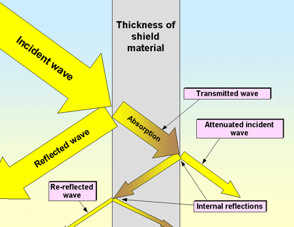
Figure 4E Reflection and absorption by a shield
In near-field regions, electric (E) fields generally have very high impedance, so are easily reflected by very thin metals, as long as they have a highly conductive surface and a low-impedance connection to the RF Reference Plane of the circuit being protected, at the highest frequencies to be shielded. But near-field magnetic (H) fields tend to have low impedance and so do not experience much reflection - their shielding relies more on absorption of the transmitted wave, and needs a suitable metal thickness to get a good SE (i.e. many skin depths at the frequency of concern, see below).
In far-field regions, ’plane’ waves have middling impedance. For instance, in air or vacuum the wave impedance is close to 377Ω (it will be lower in other media), so good SE depends upon both surface conductivity and thickness. Figure 4F illustrates how absorption improves the emissions and immunity of shielded electronic circuits.
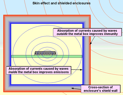
Figure 4F Absorption and shielding
At thicknesses of 0.75mm or over, and frequencies above 200kHz, most normal fabrication metals provide good SE, with excellent SE above 10MHz. Problems with shielded enclosure at such frequencies are mostly caused by apertures and cable penetrations, which are covered in later sections.
Many textbooks and free guides (e.g. [7]) describe how to calculate the SE of shielding materials from wave equations and first principles. This is a very interesting academic exercise, but the results only apply in the far-field of an EM source so may not be at all accurate in predicting SE when a shield is in the near-field of a source (see later). Also, they generally ignore the effects of apertures and cable penetrations, which almost always dominate real-life SE performance.
4.3.3 Skin effect and absorption
When a radiated wave impinges upon a conductive material it generates surface currents in the material. As the transmitted wave penetrates a shield it gives rise to eddy currents inside the shield’s material, and these can be considered to be part of the surface currents. The finite conductivity (non-zero resistivity) of the material causes these eddy currents to lose energy as heat, governing the rate of absorption of the transmitted wave. This is called the ’skin effect’ and its performance (rate of absorption) depends on frequency, and on the conductivity and permeability of the shield material.
One skin depth (δ) is the depth in the shield material at which the skin effect causes the currents caused by the impinging H field to be reduced by approximately 9dB. So a material that was just three skin depths thick would provide about 27dB of absorption to the overall SE achieved by the shield (due to the first and second reflections).
Figure 4G provides the formula for δ, and a guide graph showing copper, aluminium and a typical grade of mild steel. For copper, δ is 66/√f, and f in MHz gives δ in mm.

Figure 4G Skin depth formula and graph
Aluminium, copper, silver, gold, etc. have high conductivity and a relative permeability of 1 (the same as air), and in normal constructional thicknesses of 0.75-3mm are good at shielding any kinds of fields (E, H or EM) above 200kHz, because they achieve several skin-depths of absorption.
Mild steel is a ferromagnetic material with a relative permeability of about 300 at low frequencies, falling to 1 at frequencies above 1MHz, giving it a significantly smaller δ for frequencies below 10kHz, where it is often the better choice for shielding. Nickel is another commonly-used ferromagnetic metal, and like mild steel and all other ferromagnetic metals it loses its ferromagnetism above some frequency. Mild steel, nickel, and most/all other ferromagnetic metals have lower conductivity than good conductors like copper or aluminium, which means they have less reflectivity.
Mild steel or nickel that is plated heavily with tin can be good materials for a wide range of frequencies - the steel or nickel providing good absorption at low frequencies, and the tin plating providing good reflection. Different grades of steel (especially stainless) have different conductivities and permeabilities than mild steel, and might need to be substantially thicker for same SE.
For more information on skin depth, see [8], and Table 34-1 of [5].
4.3.4 Very low frequency shielding
Skin depth increases as frequency decreases, so skin depth becomes very important when shielding at low frequencies. As Figure 4G shows, at 50Hz even mild steel has a δ of about 2mm, so with normal constructional material thicknesses does not achieve very good SE.
Protection from very low frequency H fields is best achieved by segregation - placing susceptible devices and circuits in areas of low field strength - and also (where possible) by reducing the levels of the fields by modifying their sources so they emit less. Cathode ray tube (CRT) devices, such as used historically in oscilloscopes, televisions and computer monitor displays; photomultiplier tubes; electron microscopes; and some other devices are especially sensitive to H fields. The easiest solution for CRT displays these days, is simply to replace them with liquid crystal display (LCD) devices.
If it is necessary to shield from such fields, and the thicknesses of steel or nickel required would be impractical, special ferromagnetic metals with high values of μr, typically in the range 10,000 to 350,000 can be used, for example MuMetal®, Radiometal®, Permalloy®, etc. Designing with such metals is not about reflection and absorption, instead they are used to divert the magnetic flux away from the region to be shielded - sometimes called ’flux-ducting’.
All ferromagnetic materials can be saturated in sufficiently intense H fields, and then they don’t work very well as shields and may even get hot. For this reason a steel or high-permeability metal box placed over a mains transformer to reduce hum fields can saturate and fail to achieve the desired benefit. Often, all that is necessary is to make the box larger so it does not experience such intense H fields.
Generally speaking, the higher the permeability of the material, the lower its saturation flux density, so a common technique is to use one or more layers of low or medium permeability material spaced away from another layer of very high-permeability material. The low or medium permeability materials must be on the side facing the field, to reduce the flux density to something that the very high-permeability material can handle without saturating.
Some companies manufacture double- or triple-layer laminated metals specifically for very low frequency H field shielding purposes, and some make large shielded enclosures out of it, for example for protecting electron microscopes.
Medium and high permeability materials are usually very sensitive to handling or machining stresses. A sharp knock can cause them to lose a great deal of their permeability, whereupon they must be annealed at high temperature in a hydrogen atmosphere. So it is best to purchase such materials already fabricated and annealed by specialist manufacturers, ready for final assembly.
Another shielding technique for low frequency shielding is active cancellation, and at least two companies have developed this technique specifically for stabilising the images of CRT VDUs in environments polluted by high levels of power frequency H fields. A framework of insulated conductors is placed around the region to be protected, and audio-frequency power amplifiers drive currents in each one so as to cancel most of the H fields (measured by magnetometers) inside their protected volume. Although this is becoming less used as CRT displays are replaced with LCDs, it still finds application in areas such as electron microscopy and other H-field sensitive scientific and medical measurements.
4.3.5 SE is compromised by leakage from apertures
This section is concerned with designing and assembling to control field leakage from apertures in shields. A later section covers leakages due to cable penetrations.
It is easy to get SEs of over 100dB from quite thin metals at frequencies above 10MHz, but the SEs of all real shields are seriously compromised by the fields that leak from even tiny apertures (gaps) at seams, joints, doors, covers, etc., and also by cable penetrations. A shielded enclosure that achieves 100dB is quite costly, and usually the sort of thing used by military and other non-commercial organisations.
Control of apertures and cable penetrations is the key to achieving good SE figures - much more important at frequencies above 100kHz - than the type or thickness of the metal a shield is made from. People will often purchase a very expensive shielded enclosure, and then completely ruin its SE by failing to design its apertures and cable ports correctly, or not taking sufficient care in assembly.
A lot of information is freely available on designing shields, for example [9], [10], [11], [12], but it tends to gloss over the actual effects of apertures and cable penetrations on SE - even though a major part of the business of many of the companies that supply this helpful information is in supplying conductive gaskets which are used to limit the effects of apertures.
It is tempting to compare EM shielding with water or gas plumbing (’gaps mean leaks’) but the leakage from shield apertures does not work like that - the fields inside or outside the box do not ’squirt’ through gaps like water or gas does under pressure.
Instead, as mentioned earlier, when a field impinges upon a shielding metal, currents flow in its surface (see Figure 4F). When these ’surface currents’ encounter an aperture, they must divert from their preferred path in order to flow around it. Diverting a current creates an inductance and the H fields associated with that are in exactly the right orientation to pass straight through the aperture, which means straight through the shield material, causing the shield’s SE to be reduced.
As the surface currents flow in the inductance created by their diversion around an aperture, voltage differences are naturally generated across this inductance, appearing across the aperture. These voltage differences generate new E fields that also reduce the SE of the enclosure.
Resonances can occur that greatly amplify the leakages through the apertures at certain frequencies. When these resonant frequencies coincide with an internal frequency, such as a clock harmonic, emissions and immunity tests are more likely to be failed at those frequencies. Baseband analogue circuits are generally sensitive to noise over very wide frequency ranges (e.g. audio circuits intended to operate over 20Hz - 20kHz are generally found to be susceptible to modulated RF fields up to 500MHz at least), so resonant apertures tend to make them more susceptible at those resonant frequencies. There are two main types of resonance that affects apertures: resonances of the apertures themselves; and resonances of the enclosure’s internal cavities.
When an aperture dimension is resonant, it has a resonant gain (Q) that amplifies the E or H fields generated by the aperture’s diversion of surface currents. It is effectively a perfectly-tuned ’accidental antenna’. The conductivity of most metals is such that there is little resistive loss in a resonating aperture, so its Q can be very high, maybe 40dB or even 60dB.
Enclosure internal resonances can also have quite high values of Q, and can amplify the surface currents over areas of the shield’s internal surfaces. When one of these ’resonant hot spots’ contains an aperture, the leakage from that aperture is considerably increased at and around the resonant frequency. Both of these resonance issues are discussed later.
Because of these resonances, the SE of a shielded enclosure generally shows some fairly sharp drops around the resonant frequencies. EMC engineers use this fact to track down the causes of poor SE, by relating the wavelengths at the frequencies of the SE’s dips to the dimensions of shield apertures (e.g. seams, joints, displays, ventilation, etc.), and also to the lengths of any cables that penetrate the shield.
But SE can sometimes be seriously compromised in a non-resonant manner, over wide ranges of frequencies. I have seen dramatic levels of emissions at frequencies up to 130MHz from a hole just 4mm in diameter (intended for a plastic snap-in PCB mounting pillar) in a small PCB-mounted shield over a microcontroller. The particularly powerful near-fields associated with a certain type of microcontroller were causing significant currents to flow in the shielding can, and it was these currents being diverted around the 4mm hole in the 0V plane that were causing the high levels of emissions. The hole was acting as an accidental antenna, but neither its diameter nor the PCB-mounted shield were anywhere near resonance at 130MHz. Soldering a small brass plate over the hole reduced the emissions dramatically, and the modification for volume manufacture was simply to move the mounting pillar a little so that it did not intrude into the shielded area of the PCB.
This understanding of the true nature of shield ’leakage’ at apertures shows us that, if long narrow apertures can be aligned so that their length is aligned with the direction of the surface currents, they should leak less. Of course, this design technique requires the direction of the surface currents to be known, and for them to have one predominant direction. This can be reasonably obvious in simple situations, for example when the surface currents are mainly due to the close proximity of a current-carrying coil, but the complexity of most modern products means that computer simulations (see later) can be necessary (see later).
4.3.6 The resonant/antenna behaviour of a single aperture in the far field
All apertures in shielded enclosures behave as ’accidental slot antennas’ - accidentally radiating/transmitting EM energy through the shield and worsening a product’s emissions and immunity performance as a result. The lowest resonance of an aperture is the frequency at which its longest dimension, g (its maximum ’gap size’: either its diameter or longest diagonal) equals half of the wavelength (λ/2). Below this first resonance the efficiency of the antenna is assumed to reduce at 20dB per decade, so for g < λ/2, we generally assume that the SE of an aperture is 20log10(λ/2g) dB.
This assumption was used to draw Figures 4H and 4J, and seems to predict SE well enough to be useful in most practical situations. At least is a design tool that is better than doing nothing. Where its predications are found to be inaccurate, it may be possible to refine it following practical experiences with the technologies and construction methods used on specific products. Figure 4H uses the plot of spectrum usages + noise from Figure 4B, but in addition plots the effectiveness of the accidental antennas caused by shield apertures.

Figure 4H The accidental antenna effects of shield apertures (only up to 2.5GHz shown)
At resonance it makes little difference how wide or narrow an aperture is, or even whether there is a line-of-sight through the aperture into the enclosure. Even apertures with widths of no more than a coat of paint or film of oxide (such as are often created at joints between sheet metal parts), or that have a labyrinthine construction, still leak just as much at their resonant frequencies as similar apertures that are wide enough to poke a finger through.
Even where two surfaces that are plain metal, or have been conductively-plated are fixed together with spot-welds, screws, etc. that make good RF bonds, it should not be assumed that they have low-resistance bonds inbetween the fixing points. All spaces between fixings should be treated as apertures, with their longest dimension, g, being (at least) the pitch spacing of the fixings. Where the quality of the RF bond at a fixing is suspect, or might degrade over the life of the product, shielding design should assume a correspondingly larger aperture.
Figure 4H is useful for getting a feel for the issue of aperture leakage, but Figure 4J is more practically useful for designing shields for far-fields. It shows, for example, that for a shielded enclosure with a single aperture, achieving an SE of 40dB at 1GHz means that the largest aperture dimension should be no larger than about 1.5mm. Note that Figure 4J only applies to a single aperture, whereas most products have several apertures, reducing SE even more (see later).

Figure 4J Guide for the SE of a single aperture in the far-field
The λ/100 ’rule’ that is often used by EMC engineers when they want good performance only gives an SE of 34dB, and then only for a single aperture. Following the more commonplace λ/10 ’rule’ really only ensures that the SE will be a positive figure - that at least the shield should be better than nothing, for frequencies with wavelengths no shorter than the value of λ that was used.
Real shielding is generally constructed with numerous joints, seams, controls, displays, ventilation apertures, slots for removable storage media, etc., all of which can behave as accidentally radiating antennas unless designed accordingly. It is clearly not easy to get good SE figures even with a single aperture, and Figure 4K gives an idea of the commercial state of the art in 1997 for the enclosures for personal computers (PCs). Modern PC manufacturers have to achieve much greater SEs to much higher frequencies (e.g. to meet FCC requirements in the USA), and the fashion of fitting PCs with transparent enclosures is guaranteed to make them non-compliant with the EMC regulations of over 40 countries, and maybe even interfere with the neighbours or possibly even airplanes flying overhead. We just have to hope such fashionable people do not operate their pretty PCs too close to a hospital or other critical facility.
Sometimes enclosures are required to provide good SE performance, for instance certain military equipment might need an SE of at least 80dB from 10kHz to 18GHz, and some critical commercial/industrial products might need to be protected from EM weapons that can create fields of up to 120kV/m at frequencies around 350MHz [13]. In such cases very close attention indeed is required to the design and assembly of any/all apertures and conductor penetrations.
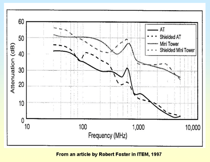
Figure 4K Some shielding effectiveness test results for PC cases
4.3.7 Multiple apertures in the far field
The leakages through apertures spaced <λ/6 apart add together more-or-less in-phase to reduce the SE of their shielded enclosure. It is usually assumed that N apertures with identical characteristics will reduce the SE of their enclosure by 20log10(N) dB, effectively causing the SE to fall by another 6dB for every doubling in the number of identical apertures, e.g. -6dB for 2 apertures, -12dB for 4, -18dB for 8, etc.
When apertures are >λ/6 apart, from some angles their leakages can phase-cancel, causing ’beaming’ of the emissions. As a result, from certain angles that depend on the frequency and the locations of the apertures on the enclosure, the SE will be better than would be achieved if all the apertures were within λ/6 of each other - and (according to simplistic assumptions) it should never be worse.
So, on balance, where multiple apertures are required, it is likely to be better for SE to spread them around an enclosure so they are as far apart from each other as possible.
The simple equations used so far in this article are very crude indeed, and this becomes obvious when we try to use them to calculate the SE of an enclosure with a regular array of apertures, as shown by Figure 4L.
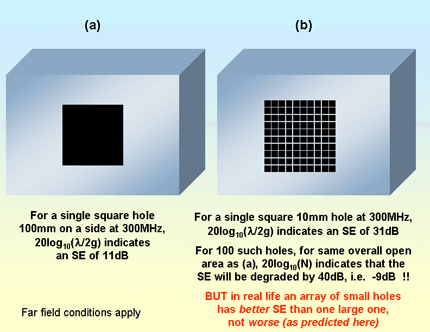
Figure 4L Strange results from simple SE equations
Figure 4L implies that it is much better to have a single large hole, than an array of smaller holes with the same overall open area. But in real-life the opposite is true: a single large hole in an enclosure has a worse SE than an array of small holes with the same overall open area. In fact, replacing large apertures with many small ones is commonly used and is considered to be a good shielding practice for ventilation apertures.
This emphasises a very important issue in shielding design - simple equations are almost useless for general use. For a shielding equation to be simple, it must have been derived from Maxwell’s equations via some huge simplifying assumptions - and so it is only appropriate for the very limited set of physical situations where those assumptions apply. Real-life shielding with real products is very complex indeed mathematically, and computer simulations (see later) are the only realistic way to predict SE with useful accuracy (say, +/-10dB).
Lacking a computer simulator, my approach is to design so that shielding can quickly and easily be improved, so that if the lowest-cost design that it was hoped would pass the emissions or immunity tests turns out not to be good enough in practice - the SE can be improved in minutes by fitting components (such as conductive gaskets and/or PCB shielding cans, already designed and samples obtained) without any redesign.
There are some simple shielding design tools freely available via the Internet, for example [14], [15] and [16], but I do not know how accurate they are at predicting real-life SE. For example, [14] uses similar simple equations to those above.
As it happens, there is a simple shielding formula that is supposed to apply specifically to the ’array-of-small-holes’ example above. It says that where an otherwise perfectly shielded enclosure has a single square hole, replacing that hole by a grid of smaller square holes within the same outline (as shown by Figure 4M) improves the SE by S dB, where.
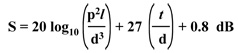
- where. λ = the length of the side of the original square hole
g = the side of the smaller square holes
p = the pitch (spacing) of the smaller holes
d = the thickness of the shield material
Figure 4M Reasonable SE predictions from an equation derived for the specific situation
This guide equation only works when g < λ/6 at the highest frequency of concern. If small round holes are used instead of square ones, g represents their diameter and S is 3dB higher. Figure 4M shows that applying this formula to an example similar to Figure 4L, the SE should be improved by about 25dB. It is difficult to say whether this will be a very accurate prediction for a real product, but at least it correlates better with real-life shielding behaviour.
The above equation only applies where the array of holes fits within the outline of the original single large hole. This means that, because of the area taken up by the metal grid between the holes, the open area of the array is less than that of the single large hole. Increasing the number of holes to achieve the same open area, e.g. for ventilation purposes, will clearly reduce the SE somewhat, but the equation does not cover this.
4.3.8 Cavity resonances and aperture leakage
As mentioned earlier, an enclosure’s internal cavity resonances can cause an aperture to leak (emit) to a much greater degree than it would normally, if the aperture lies in a region where the surface currents are being amplified by a cavity resonance inside the enclosure itself (a ’hot spot’). These resonant frequencies are governed by the enclosure’s internal dimensions, rather than by the dimensions of the aperture.
Figure 4N shows the simple equation typically used to estimate cavity resonances. Because a shielded enclosure has a low impedance at all of its boundaries, it can only experience cavity resonances that have integer (whole) numbers of half-wavelengths, at frequencies given in MHz by f = 150√{(l/L)2 + (m/W)2 + (n/H)2}, where: l, m and n are integers (0, 1, 2, 3 etc.) representing the number of half-waves that fit between the parallel metal surfaces along any of the three axes, and L, W and H are the box’s length, width, height respectively, in metres. (If the dimensions are stated in millimetres, the resonant frequencies are given in GHz.)
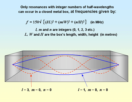
Figure 4N Resonances and ’standing waves’ caused by reflections inside a metal box
Figure 4N sketches the field distributions for two solutions of the above equation, one for what is known as the (1,0,0) mode, in which l =1 half-wave, m = 0, and n = 0, and one for the (3,0,0) mode in which l =3 half-waves, m = 0, and n = 0. These examples show the ’standing wave’ patterns for the E field distributions at these resonant frequencies. The waves are not really stationary, they are actually ricocheting back and forth between the two metal sides of the box at the speed of light, but unless we have very fast instruments we see them as if they are stationary.
It is possible to imagine very complex modes, such as (27,13,19), but in the main we are interested in simple resonant modes such as (x,0,0), which is side-to-side, (0,x,0), which is half-wave front-to-back and (0,0,x), which is top-to-bottom. A significant resonance is the (1,1,1) mode - which gives us the lowest internal resonant frequency, between opposing corners, along the three-dimensional diagonal.
Figure 4P shows an example of a three-dimensional field solver plotting the E field strengths inside a shielded box at one of its resonant frequencies (which appears to be its (3,0,0) mode). The field leakage through a small aperture in the box can clearly be seen.
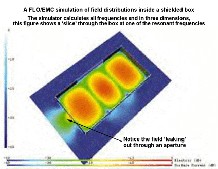
Figure 4P Examples of real-life cavity resonances
Adding metalwork, printed circuit boards, cables, etc., inside a box affects its resonant frequencies, generally they make its resonances lower in frequency, as in the example shown in Figure 4Q. They can also add new resonant frequencies.
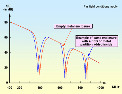
Figure 4Q Examples of cavity resonance frequencies being reduced by box contents
Resonant hot spots within the volume of an enclosure can sometimes have significant effect on signal integrity, due to the amplification of crosstalk phenomena at the resonant frequencies, between cables and/or PCBs. Careful design will ensure no especially sensitive or noisy components (or conductors associated with them) are placed near a hot spot, unless they are appropriately shielded or filtered.
4.3.9 Near-field leakages through apertures
So far we have assumed that the source was so far away that its EM radiation was plane waves, i.e. the shield was in the far-field of the radiating source - the usual situation when trying to protect electronics from external RF sources (to improve immunity).
But when using shielding to reduce emissions from a product, the shield is usually in the near-field of the source - and the SE from plane wave assumptions can be very wrong indeed, especially at lower frequencies. The closer the RF source is to the apertures, the worse the SE. Very significant amounts of leakage can occur, especially at low frequencies, even through arrays of very small apertures that have very low SE for plane (far-field) waves, see [17] for more detail.
Figure 4R sketches the E and H fields around an aperture, indicating that they are associated with regions of reduced SE, where it would be inadvisable to locate noisy or sensitive components or conductors.
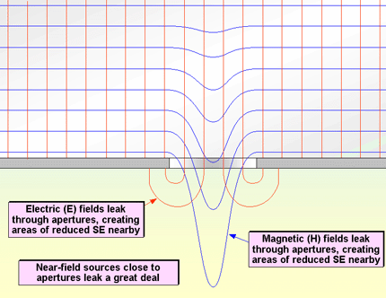
Figure 4R SE for near-fields is less when sources are near an aperture
4.3.10 Designing to reduce aperture leakages
Eliminate apertures. Only allow apertures that are necessary for the function of the product.
Reduce aperture size. Do not allow apertures to be any larger than necessary. Break any necessary apertures up into smaller ones, as shown by Figure 4M, to make their resonant frequencies much higher than the highest frequency of concern. Where there are long seams or joints between metal structures, they should be electrically connected using direct metal-to-metal bonding techniques at regular intervals along the seam or joint.
Figure 4S shows the principles of direct metal-to-metal RF bonding, which should be used where bonds cannot be welded. It is generally bad EMC practice to rely on the fixing device (e.g. the self-tapping screw, in Figure 4N) to make the electrical bond (although this is unfortunately quite a common practice). Apart from the poorer RF performance of the bond, one of the problems with relying on the fixing device to make the bond is that company component buyers might source fixings with non-conductive plating, destroying SE completely.

igure 4S Principles of direct metal-to-metal RF bonding
Flexible conductive gaskets, often called EMC gaskets, are very valuable for reducing aperture sizes, especially where apertures must be long - for example around removable covers, doors, shielded windows, shielded ventilation panels, etc. Gaskets and gasketting methods are discussed in their own chapter, later.
Spread necessary small apertures as far apart as possible. For frequencies at which the spacing is larger than λ/4, some reduction of emissions will occur at some angles. To have any significant effect at 600MHz (where λ is 500mm), the spacing should be >125mm. It is even better if the necessary apertures can be placed on different sides of the enclosure. Don’t expect large improvements from this technique.
Reduce near-field leakages. Where it is impractical to completely fill an aperture with a conductive gasket, to reduce the impact of near-field leakages from reducing the enclosure’s SE, make sure that all wires, cables, PCB traces, components, etc. are not near an aperture. This is especially important for any conductors or components that are especially noisy (e.g. flyback inductors in switch-mode power supplies; microprocessors, PCB traces carrying high-rate data), and also important for any that are especially sensitive (e.g. analogue amplifiers, microprocessors, PCB traces carrying high data rate signals).
As far as I know there are no simple equations that can be used, but a crude guide might be that for an SE of more than 40dB at any frequency, the spacing between a conductor or component and an aperture should generally be at least 1.5 times the longest dimension of the aperture (i.e. its diameter or longest diagonal). Larger spacings are recommended, especially at lower frequencies. See [17] for more on this, noting that the coupling coefficient it uses could be considered to be the reciprocal of SE, which means simply reversing the sign from negative dB to positive dB.
Make shielded cavities smaller. The aim of this method is to make the cavities inside the shielded enclosure smaller, so that they each resonate at a much higher frequency than is cared about. If the highest frequency of concern was 1GHz, cavities with longest 3-D diagonals of less than 125mm are required. This is another reason why using many small shielding cans on PCBs can be more cost-effective than an overall shielded enclosure. Often, a single large screening can is subdivided inside to create many smaller cans, to save assembly time (see the section on PCB shielding, later).
For example, Figure 4T shows one side of a shielded plastic enclosure for a telecommunications product, which has been subdivided into many smaller shielded internal volumes by ribs in the plastic moulding with form-in-place soft conductive gaskets extruded by robotic assembly machines along the ribs. Such multi-compartmented shielded enclosures can also be a great help for signal integrity - separating different circuits within a product more effectively from each other and reducing the crosstalk between them.

Figure 4T Example of a multi-compartmented shielded enclosure
Damp cavity resonances with absorber. Where a cavity’s resonances cannot be made small enough to resonate at a higher frequency than is cared about (see above), the Q of cavity can be damped to reduce emissions by a useful degree with two basic kinds of materials:
- Carbon-loaded elastomer, usually foam, which absorbs energy from the E-field and so is usually placed away from the walls of the enclosure.
- Ferrite-loaded elastomer, usually solid, which absorbs energy from the H-field and so is usually placed close to the walls of the enclosure.
These materials come in various thicknesses, with various proportions of carbon or ferrite filler. The types that provide more damping and/or operate at lower frequencies, are generally heavier and more expensive. Typically they only provide useful amounts of damping at frequencies above a few hundred MHz. These materials are available in sheet form, with or without self-adhesive backing, and also available in die-cut preforms as shown in Figure 4U.
Some manufacturers (e.g. Laird Technologies) offer ’absorber cans’ as standard parts for shielding on PCBs, supplied with absorber already fitted to an inside surface.

Figure 4U Examples of die-cut RF absorber materials
Randomise the cavity resonances. Where a cavity’s resonances cannot be made small enough to resonate at a higher frequency than is cared about (see above), SE can be improved by careful design of enclosure shape, and aperture shape and location. Regular shapes have modes that resonate at the same frequencies, making the overall Q at those frequencies even higher.
For example, if a metal box is 1m long, 0.5m wide and 0.25m high, all of its three dimensions will resonate at 600MHz: four half-wavelengths along its length, two half-wavelengths across its width, and one half-wavelength between its top and its bottom. So at 600MHz (and also at 1.2, 1.8, 2.4,.etc. GHz) the Q of the cavity will be much larger than is usual for a cavity resonance and aperture leakages can be expected to be higher as a result.
The solution is to avoid regular shapes. A common approach is to arrange the length, width and depth in the ratio 3:4:5, which is not bad but could be improved upon, for example by using irrational numbers for the ratios, avoiding numbers that are too close to simple ratios (such as √2 because it is too close to 1.25) - especially if the lowest-cost product is required. The ’golden mean’ (1.618.) may be a suitable choice - not least because it gives a pleasing aspect to the human eye, as architects and artists have known for thousands of years. If using circular shapes, avoid shapes with a single radius of curvature such as cylinders or spheres.
Another useful method is to avoid parallel metal surfaces. In the days when mechanical designs were made using drawing boards, set-squares and compasses, and metal parts were cut from sheet and folded by hand, it was hard to avoid regular shapes such as rectangles and circles. But these days we have much more flexibility and can more easily design, manufacture and assemble enclosures using shapes based on non-parallel planes and curved sections with smoothly-varying radii.
Even where the external structure must be rectilinear with parallel sides, or (worse still) have a square cross-section or be a cube, this does not necessarily mean that the internal metal structures forming the shield(s) must be as regular.
It is important to remember that internal resonances are modified by internal conductive and dielectric structures, so to reliably obtain benefits from this approach requires early-stage design simulation of the shielded enclosure, based upon its likely apertures (e.g. seams, joints, doors, displays, ventilation, etc.) and the shapes, sizes and locations of the objects it is likely to be contain (e.g. trays, shelves, brackets, PCBs, heatsinks, cables, etc.).
Careful design of an enclosure can help achieve the lowest-cost product that still complies with EMC regulations and is sufficiently reliable in real-life use - by helping to reduce the cost and weight of the shielding and filtering measures required. But, as is usually the case where lowest-cost products are required, this requires more design resources, in both expertise and time. The use of computer simulators (see later) is an excellent way to add field-solving expertise without having to learn field theory, and commercially available computer simulators running on desktop PCs can easily predict field distributions for real-life products that even the most egg-headed EM field theory expert would not attempt.
The ’dirty box’ technique. Where a hole must be cut in a shield, for example for panel-mounting a control, lamp indicator, etc. - but the component to be thus mounted does not need to be shielded - a secondary shielding box can be used, often called a ’dirty box’ (the ’clean box’ is the inside of the shielded enclosure). Figure 4V shows the important points of this versatile technique.
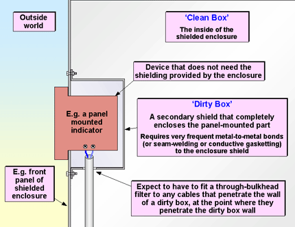
Figure 4V Examples of the use of the ’dirty box’ method
Notice especially that the dirty box must be treated like any other shielded enclosure - with careful design of its apertures (see above) and cable penetrations (see below). Bulkhead filters may be needed for all cables penetrating the dirty box walls, and should be allowed for in the design in case they turn out to be needed (’anti-Murphy’ design techniques, see earlier). These filters often only need high attenuation above 100MHz, so can be small, and may even be able to be replaced with ferrite chokes (such as those shown in Figure 3G of [18]) mounted on the cable very close to the point where they penetrate the dirty box.
Techniques for large apertures. Where apertures must be large, for example for doors, covers, display screens, etc., and the ’dirty box’ technique is not appropriate, there are a number of techniques that have been developed to help achieve good SE.
- Waveguides below cutoff
- Shielded windows for displays
- Shielding membrane switch panels
- Shielding ventilation
- Gasketting with conductive gaskets
The first three in the above list are described in the next three sections, but conductive gasketting is a fundamental technique that can be used with all of the other aperture-control techniques, so it is given its own chapter towards the end of this article.
4.3.11 Waveguide-below-cutoff techniques
Waveguides have a cut-off frequency below which they cannot be used to ’pipe’ EM waves from one place to another. In fact, their attenuation factor for frequencies below about 60% of their cut-off frequency can be very much higher than for a comparable aperture in a shielded enclosure, and this principle is sketched in Figure 4W.
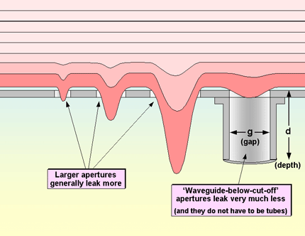
Figure 4W Waveguides used below cutoff leak much less than comparable apertures
The cut-off frequency of a waveguide occurs when its maximum aperture dimension, g (its diameter or longest diagonal, as before) is half a wavelength, so in air or vacuum: fcutoff = 150/g MHz when g is specified in metres. If g is given in millimetres instead, this formula gives the cutoff frequency in GHz.
Below its cutoff frequency, the attenuation of a single waveguide depends on its ratio of depth (d) to longest aperture dimension (g). For frequencies that are less than about 0.6 of the cutoff frequency, a waveguide has a constant attenuation of approximately {27 d/g} dB, so...
- d/g = 2 gives SE = 54 dB
- d/g = 3 gives SE = 81 dB
- d/g = 4 gives SE = 108 dB
These figures indicate very much lower leakages, and therefore much higher SEs, than apertures with the same dimensions but a negligible value of d, as shown by the examples in Figure 4X.
Designing any necessary apertures in a shielded enclosure as waveguides-below-cutoff will very significantly reduce their impact on SE. To achieve these benefits, their cutoff frequency should ideally be at least double the highest frequency of concern.

Figure 4X Estimated SEs for some example waveguides-below-cutoff
It is important to note that, just as for any aperture, passing any conductor through a waveguide-below-cutoff will completely ruin its attenuation and therefore ruin the SE of the shielded enclosure. There are no exemptions to this rule, regardless of the function of the conductor (e.g. mouse or keyboard cables, draw wires in fibre-optic cables, waste water).
However, waveguides-below-cutoff are very useful indeed for passing non-conductors (dielectrics) into or out of shielded enclosures - as long as the effect of their relative permittivity (dielectric constant, εr) in reducing the cutoff frequency is taken into account.
So far, this discussion, and Figure 4X, has assumed that the waveguide is filled with air (or vacuum), but filling with any dielectric with an εr greater than unity (e.g. oil, distilled water, glass, plastic) results in a reduced cutoff frequency given by: fcutoff = 150/(g√εr) MHz (for g in metres). For mixed dielectrics - use the average value of εr over the cross-sectional area to estimate the new cutoff frequency.
[4] makes the point that it is much better for EMC to use fibre-optic cables than ordinary conductive cables, and that although the component and material costs of fibre-optic interconnections may be higher than copper, the overall cost of manufacture, reduced warranty costs and increase customer satisfaction often means that they achieve an overall financial benefit. In addition to these EMC benefits, metal-free fibre-optic cables can be passed through the walls of shielded enclosures, using waveguide-below cutoff techniques to have a negligible effect on SE.
Many types of fibre-optic bulkhead connectors or couplers function as very effective waveguides-below-cutoff up to at least 10GHz. The bulkhead connector must be metal, and it must make a 360ø metal-to-metal bond with the shield around the hole cut for it in the shield’s wall, following the RF bonding principles illustrated in Figure 4S. The optical fibre has a high value of εr so the cutoff frequency will be lower than would be expected simply from consideration of the inner diameter of the metal connector or coupler.
Waveguides-below-cutoff do not have to be tubes - their shapes are limited only by the imaginations of mechanical designers and constraints of the products. For example, Figure 4Y shows that using thicker shield materials (e.g. 3mm instead of 1mm) with apertures that have a comparable (or smaller) longest dimension, g, reduces the leakages through the apertures significantly, because they start to behave as waveguides-below-cutoff.
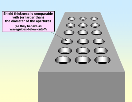
Figure 4Y Aperture longest dimensions comparable with shield thickness
The 27(d/g) term in the earlier equation for replacing a large aperture with a number of smaller ones represents the contribution from the waveguide-below-cutoff effect. For the example shown in Figure 4M it only added 2.7dB to the improvement in SE, because the shield thickness d was 1mm, whilst the sides g of the small square apertures were 10mm. But if d had been 3mm and g 5mm, its contribution to improving the SE of the enclosure would have increased from 2.7dB to a more useful 16dB.
An obvious use for this technique is for ventilating shielded enclosures, and it can be developed much further by the use of ’honeycomb metal’. An example of honeycomb metal, and of some panels made from it, are shown in Figure 4Z. Honeycomb metal is made of small tubes with hexagonal cross-section, with a d (length) very much smaller than their g (largest aperture dimension), giving a d/g ratio that often exceeds 6, for very low leakage indeed.
Small holes are not very efficient for ventilation, especially when made in thick plates of metal (as shown in Figure 4Y). Where ventilation is critical, achieving the same airflow rates and pressures as larger holes, often requires more 'open area' for the smaller holes - which tends to reduce the SE benefits of small holes in thick metal. The hexagonal tubes in honeycomb metals have very thin walls, so for ventilation they behave almost as well as a single large aperture, whereas for SE they behave like a large number of very-high-attenuation waveguides-below-cutoff.
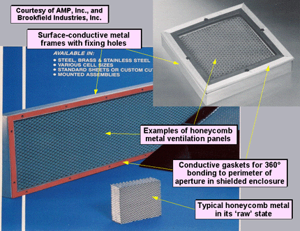
Figure 4Z Some examples of using honeycomb metal for shielding
Honeycomb metal panels can also be used to shield apertures where optical energy is emitted, (e.g. lamps, lasers, etc.) and have even been used to shield display screens - which can then only be seen from immediately in front (which can have benefits in security-conscious applications). Fibre-optic cables can also be passed through the honeycombs, as long as the cables are totally metal-free.
Metal honeycomb panels used to be costly items, with large NRE (non-recurring engineering) charges that made prototypes extremely expensive. But modern manufacturers use computer-controlled robotic manufacturing tools, so the only NRE is that needed to capture their 3-D drawings. About two years ago I was quoted around œ150 for a prototype honeycomb panel about 300mm square, similar to the ones shown in Figure 4Z. Ten years ago that figure would have been about ten times larger.
To be effective in shielding applications, honeycomb metal panels must have a metal frame with good surface conductivity, with sufficient stiffness and enough fixing holes to correctly compress a conductive gasket around its entire perimeter - to avoid creating additional apertures that would degrade SE. Alternatively, they can be glued in place using conductive adhesives.
Honeycomb metal is naturally very light and stiff, which helps it to compress conductive gaskets correctly without requiring large number of fixings (see later for gasket design). The honeycomb tubes are glued together, so for the best shielding performance use panels that were plated with a low-conductive finish after assembly.
Figure 4AA shows a recently-developed shielding product - honeycomb plastic with an overall conductive plating, and a conductive elastomer gasket bonded around its perimeter. It doesn't have the rigidity and strength of honeycomb metal, but it weighs less and should also cost less whilst having similar attenuation characteristics to honeycomb metal.
Another application of the waveguide-below-cutoff technique is simply to provide greater overlaps at metal seams and joints, as shown in the example in Figure 4AB. This method does not really use waveguides, so the normal waveguide-below-cutoff theory and equations no longer apply - but in practice these forms of construction do seem to behave in a similar manner (which we might call 'pseudo-waveguide-below-cutoff'), which is why it is included in this section.

Figure 4AA Examples of plastic honeycomb shielding material

Figure 4AB Joint overlaps comparable with fixing pitch
I was once testing a product constructed rather like Figure 4AB with close-field probes to determine the cause of its enclosure's poor shielding of its internal 900MHz oscillator. The enclosure had a flat metal lid screwed onto flanges that were about 8mm wide, except along one edge where the flange was 25mm wide (for reasons that are not relevant). The lid was held down with screws located every 60mm around its perimeter. The close-field probe found uniformly high levels of emissions all around the three sides with the 8mm flanges, but 10dB lower emissions all along the edge with the 25mm flange.
Assuming the fixings and flanges create waveguides (which they do not), the simple waveguide-below-cutoff formulae above show that the cutoff frequency of the 60mm fixing pitch is 2.5GHz, so 900MHz is low enough to fall in the 27(d/g) dB region - which predicts that the 25mm flange should have 12dB attenuation, whilst the 8mm flange has 3.6dB. The difference between these two calculated figures is 8.4dB, much closer to the 10dB that was measured with the close-field probes than could have been hoped for (or is usually the case) when trying to compare simple EMC equations with practice, especially using close-field probing. Close-field probing is a very valuable technique for developing and fault-finding shields, and also for checking their assembly in series manufacture, for more information see Parts 1 and 2 of [19].
Reducing the longest aperture dimension, g, means adding more RF bonds, but assembling large numbers of fixings adds to assembly time and adds to the cost of manufacture. Small conductive gaskets, such as individual spring fingers, can be used instead, to make the necessary RF bonds. Sufficient mechanical fixings will still be required - to compress the pieces of gasket, if for no other reason - but because this method does not use long lengths of gasket it avoids the mechanical difficulties of providing very large amounts of pressure (see the section on gaskets, later).
Figure 4AC shows an example of the addition of individual spring finger gaskets to a cover plate, to improve the SE of the enclosure by breaking four long apertures up into 12 shorter ones (smaller values of g) to improve SE without adding more fixings. The visible surfaces of the product might be painted or anodised, but the areas that the spring fingers contact must be highly-conductive surfaces - their materials and plating selected for low corrosion in their intended operating atmosphere (see later) so that good SE is maintained for the life of the product.
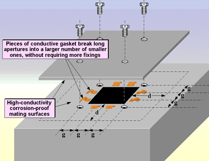
Figure 4AC Example of reducing the aperture dimension g with conductive gaskets
Spring fingers are generally supplied in strips, but can be purchased singly or cut off from a strip. They can sometimes be formed in the metal of the enclosure itself, for example by a 'semi-punch' process. Many other types of strip gasket can be cut with scissors to use as 'dots', but types that might shed conductive particles from cut edges should be avoided. Some EMC gasket manufacturers make products especially for the purpose shown in Figure 4AC, e.g. 'fuzz buttons' (from Tecknit) or 'gasket dots'.
Where a shield's mating part is a PCB, spring fingers and many other types of RF bonding components are available in surface-mounted styles, such as Gore-Shield SMT. Suitable components include anything that is volume- or surface-conductive, and area contacts on both sides are preferred over point contacts. However, it is very important to avoid any components that rely on a wire bond, especially if it is a spring - such components have too much inductance to make good RF bonds.
Figure 4AD shows an example of a shielded enclosure design that uses pseudo-waveguide-below-cutoff techniques like those of Figures 4AB and 4AC, with a single quarter-turn plastic fastener used to retain the cover. I know of no product like this, it is just an example to show what is possible.
The overlap at the seam between the cover and the base has been increased by making the cover a five-sided box instead of a flat plate, so that when it is assembled onto the base the (pseudo-) waveguide depth, d, comprises the flange plus most of the height of the enclosure. Spring fingers along the flanges make contact with conductive surface inside the cover, giving a value of g that is much less than d, hence very good attenuation and low field leakage. The five-sided metal cover is naturally very stiff, helping to ensure correct compression of the gasket pieces. The gap between cover and base could be used for ventilation (would probably need an air-mover).

Figure 4AD Joint overlaps comparable with fixing pitch
One of the problems with covers fitted with multiple fixings, such as that shown in Figure 4AB, can be that after a year or two's use in the field most of the fixings can be missing, and the enclosure's SE sadly degraded. This is especially a problem where covers must be removed for maintenance - it is just too tedious to bother putting all the screws back in, with the correct torques. The design shown in Figure 4AD solves this by using a single quarter-turn plastic fixing that allows the cover to be removed and replaced very quickly indeed. Such plastic fasteners are also available in 'captive' styles, so that they cannot be lost (unless the cover is lost with them). And of course their positive 'snap-in' action makes it easy to ensure that the gasket pieces are optimally compressed over many years of operation.
There are many more types of design that use waveguide-below-cutoff techniques to achieve very good SE for enclosures with the lowest cost-of-manufacture - but a common thread is that they must be designed-in from the start of the project. It is generally impractical to try to use these techniques to 'fix' non-compliance problems late in a project, or to solve problems due to interference in the field.
Very many electronic manufacturers allow their designers to focus only on functionality and cost, ignoring all else, leaving EMC performance to the end of the project - when a pre-production prototype or early production unit are sent to an EMC test laboratory to "get their CE mark". Some project managers have even been known to insist that their designers behave in this financially risky manner. When the test is not passed, there is a scramble to fix the problem quickly using whatever it takes to get to market on time. Unfortunately, by that time the design freedom is very limited, and modern digital electronic technologies are increasingly making traditional post-design 'fixes' (ferrite beads, copper tape, adding capacitors, etc.,) ineffective. So it is increasingly likely that after months of trying everything, the only solution can be a complete redesign with associated huge costs and huge financial risks.
It makes much better financial sense to employ the efficient, cost-effective, and well-known EMC techniques discussed in this series of articles, such as waveguide-below-cutoff methods, right from the start of a project.
4.8 References
[1] Keith Armstrong, "Design Techniques for EMC", UK EMC Journal, a 6-part series published bimonthly over the period February - December 1999. An improved version of this original series is available from the "Publications & Downloads" page at www.cherryclough.com
[2] The Institution of Engineering and Technology (IET, was the Institution of Electrical Engineers, IEE), Professional Network on Functional Safety, "EMC and Functional Safety Resource List", from the "Publications & Downloads" page at www.cherryclough.com
[4] Keith Armstrong, "Design Techniques for EMC, Part 2 - Cables and Connectors", The EMC Journal, May and July 2006, from the "Publications & Downloads" page at www.cherryclough.com
[3] Keith Armstrong, "Design Techniques for EMC, Part 3 - Filtering and Suppressing Transients", The EMC Journal, September and November 2006, and January 2007, from the "Publications & Downloads" page at www.cherryclough.com
[5] John R Barnes, "Robust Electronic Design Reference Book, Volume I", Kluwer Academic Publishers, 2004, ISBN: 1-4020-7737-8. See Chapter 34 for shielding and shielding design.
[6] Keith Armstrong, "Design Techniques for EMC, Part 0 - Introduction, and Part 1 - Circuit Design and Choice of Components", The EMC Journal, January 2006 pp 29-41, plus March 2006 pp 30-37, available from http://www.compliance-club.com.
[7] "Shielding Design and Calculation", Ron Brewer, Laird Technologies Tech Notes #105, from www.lairdtech.com
[8] RF Caf‚, Skin Depth, http://www.rfcafe.com/references/electrical/skin_depth.htm
[9] "Shielding Methods", Chomerics, http://www.chomerics.com/tech/Shielding_methods.htm
[10]"EMI Shielding Engineering Handbook", Chomerics, available from: http://www.chomerics.com/tech/Shielding_methods.htm
[11]The chapter entitled "EMI Shielding Theory & Gasket Design Guide" in the Chomerics "EMI Shielding Engineering Handbook", available from: http://www.chomerics.com/products/emi_lit_contents.htm
[12]"Technical Notes", Laird Technologies, technical information and guidance on shielding and gasketting, available from: http://www.lairdtech.com/pages/catalogs/emi.asp (scroll down the page to the "Technical Notes" section).
[13]William A. Radasky, "The Threat and Detection of Electromagnetic Weapons at Airports and on Aircraft", 2005 IEEE Conference on Technologies for Homeland Security, Boston, Massachusetts, 26 April 2005, available from http://.ieeexplore.ieee.org
[14]"An Aperture Attenuation Modeling Program to Determine Shielding Effectiveness of Printed Circuit Board Shields and Other Enclosures", free spreadsheet from MAJR Products, Inc., download from http://www.majr.com/freetool.htm
[15]A free SE calculator (for far-field SE): www.emc.york.ac.uk/examples/screening/index.html
[16]A free SE calculator (for far-field SE): http://www.amanogawa.com/index.html (click on 'EMC/EMI', then 'Java Applets', then on 'Shielding Effectiveness')
[17]Shabista Ali, Daniel S Weile, Thomas Clupper, "Effect of Near Field Radiators on the Radiation Leakage Through Perforated Shields", IEEE Transactions on EMC, Vol 47, No. 2, May 2005, pp 367-373.
[18]Keith Armstrong, "Design Techniques for EMC, Part 3 - Filtering, and Suppressing Transients", The EMC Journal, September and November 2006, January 2007, available from http://www.compliance-club.com
[19]Tim Williams and Keith Armstrong, "EMC Testing", a series in seven parts published in the EMC & Compliance Journal 2001-2, available from the 'Publications & Downloads' page at www.cherryclough.com.
4.9 Acknowledgements
I am very grateful to the following people for suggesting a number of corrections, modifications and additions to the first series published in 1999 [1]: Feng Chen, Kevin Ellis, Neil Helsby, Alan Keenan, Mike Langrish, Tom Liszka, Tom Sato, and John Woodgate.
Eur Ing Keith Armstrong CEng MIEE MIEEE
Partner, Cherry Clough Consultants, www.cherryclough.com, Member EMCIA
Phone: +44 (0)1785 660 247, Fax: +44 (0)1785 660 247,
keith.armstrong@cherryclough.com; www.cherryclough.com