Advanced PCB design and layout for EMC. Part 1 – Saving time and cost overall
This is the first in a series of eight articles on good-practice EMC design techniques for printed circuit board (PCB) design and layout. This series is intended for the designers of any electronic circuits that are to be constructed on PCBs, and of course for the PCB designers themselves. All applications areas are covered, from household appliances, commercial and industrial equipment, through automotive to aerospace and military.
These PCB techniques are helpful when it is desired to…
- Save cost by reducing (or eliminating) enclosure-level shielding
- Reduce time to market and compliance costs by reducing the number of design iterations
- Improve the range of co-located wireless datacomms (GSM, DECT, Bluetooth, IEEE 802.11, etc.)
- Use very high-speed devices, or high power digital signal processing (DSP)
- Use the latest IC technologies (130nm or 90nm processes, ‘chip scale’ packages, etc.)
The topics to be covered in this series are:
- Saving time and cost overall
- Segregation and interface suppression
- PCB-chassis bonding
- Reference planes for 0V and power
- Decoupling, including buried capacitance technology
- Transmission lines
- Routing and layer stacking, including microvia technology
- A number of miscellaneous final issues
A previous series by the same author in the EMC & Compliance Journal in 1999 “Design Techniques for EMC” included a section on PCB design and layout [1], but only set out to cover the most basic PCB techniques for EMC – the ones that all PCBs should follow no matter how simple their circuits. This series is posted on the web and the web versions have been substantially improved over the intervening years [2]. Other articles by this author (e.g. [3] [4]) have also addressed basic PCB techniques for EMC. This series will not repeat the basic design information in these articles – it will build upon it.
Like the above articles, this series will not bother with why these techniques work, they will simply describe the techniques and when they are appropriate. But these techniques are well-proven in practice by numerous designers world-wide, and the reasons why they work are understood by academics, so they can be used with confidence. There are few techniques described in this series that are relatively unproven, and this will be mentioned where appropriate.
Table of contents for this part
1 Reasons for using these EMC techniques
1.1 Development – reducing costs and getting to market on time
1.2 Reducing unit manufacturing costs
1.3 Enabling wireless datacommunications
1.4 Enabling the use of the latest ICs and IC packages
1.5 Easier compliance for high-power DSP
1.6 Improving the immunity of analogue circuits
2 What do we mean by “high speed”
3 Electronic trends, and their implications for PCBs
3.1 Shrinking silicon
3.2 Shrinking packaging
3.3 Shrinking supply voltages
3.4 PCBs are becoming as important as hardware and software
3.5 EMC testing trends
4 Designing to reduce project risk
4.1 Guidelines, maths formulae, and field solvers
4.2 Virtual design
4.3 Experimental verification
5 References
1 Reasons for using these EMC techniques
Most professional circuit and PCB designers would love to employ all of the good EMC techniques described in [1] - [4] and this series, but are often prevented from doing so by project managers and other managers who only see these techniques as wasted time and added cost.
Sometimes it is the manager of the PCB layout department who prevents the use of good EMC techniques, usually claiming that the product cost-to-make will increase, but often really because they have become familiar with their existing PCB design rules and bare-board manufacturers and don’t want to make the effort to change.
This section will show that such management approaches are completely the opposite of what is really required these days for success in the design and manufacture of electronic products of any type, in any volume.
PCBs have continually been getting more high-tech and costly ever since they were first invented, and they will continue along this path for ever. In a few years time microvia PCBs with more than 8 layers and embedded capacitance will be the norm. It is a tough commercial world for everyone these days, and companies that don’t keep up with PCB technology will be left in the dust of those that do.
1.1 Development – reducing costs and getting to market on time
Even if a PCB has no nearby wireless datacommunications antennas, and even if it does not use high-speed devices or signals, these PCB techniques can save time and money by reducing the number of iterations it takes to get the circuit working with its full performance specification. This is because many EMC techniques are also signal integrity techniques. In fact, good PCB design for EMC goes beyond the requirements for signal integrity; so a PCB that is designed using good EMC techniques generally has excellent signal integrity.
The author originally developed the PCB design techniques described in [1] - [4] over ten years and three companies in the 1980s to enable powerful digital processing, sensitive high-specification analogue circuits, and switch-mode power converters to share the same enclosure, even the same PCB, without compromising the analogue performance at all. Projects that used to require 10 or more design iterations could use these techniques to meet their performance specifications on the first PCB prototype. During the 1990s it was found that these techniques also achieved excellent compliance with EMC Directive test standards, without requiring high-specification enclosure shielding, sometimes without any shielding at all.
Good EMC design techniques are good signal integrity techniques, for both analogue and digital circuits. This means more predictable project timescales with fewer three-cornered arguments between the circuit, PCB and software designers as to whose fault it is that the performance falls short of its specification.
However, there are still very many companies that do not employ the techniques described in [1] - [4], never mind the advanced PCB techniques described here. This appears to be because they don’t realise that the true cost of a design modification increases rapidly as a project progresses. People only tend to see the obvious costs of the modification (the hours spent, the cost of another prototype PCB, etc.) which are the same whatever stage the project is at, but Figure 1A gives an idea of how the real cost of a modification varies during the project timescale.
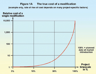
Of course, once a design iteration causes a delay in the market introduction the true costs of that modification can be astronomical. This issue is much more important than it was even ten years ago, due to the very short product lifetimes now being experienced for almost every application area. Some cellphone and computer industries already have product lifetimes of 90 days or less, but it is increasingly likely that for even quite ordinary products and equipment, being 6 months late to market can mean no market at all – with the consequent loss of all the investment in the project. For some debt-financed companies, the loss of investor confidence caused by a late market introduction can lead to the loss of the company.
So it is not too exaggerated a claim to say that good PCB design and layout techniques are a valuable financial tool and competitive weapon. The section below on ‘trends’ should make this claim even more clear.
1.2 Reducing unit manufacturing costs
1.1 above dealt with project costs, but unit manufacturing costs also benefit from the use of good EMC techniques at the level of PCB design and layout.
A general rule of thumb is that the true costs, in manufacture, of controlling EMC increases tenfold for each higher level of assembly. So the lowest-cost place to control EMC is in the design of the ICs and semiconductors. Achieving the same EMC performance at PCB level costs about ten times more than if it could be done in the IC. And if implemented at product enclosure level the true costs of achieving the same EMC performance are ten times higher again, as shown by figure 1B.

Few designers have as much control over the EMC characteristics of their ICs as they would like. Most are stuck with using commodity ICs with no EMC controls at all (in fact, some of them seem to have been designed to maximise EMC problems). FPGA designers, and especially ASIC designers, have a greater degree of control of the EMC characteristics of their devices – but even so there are limits to what current technology can achieve.
However, as subsequent parts of this series will show, it is possible to completely control all aspects of EMC (except for direct lightning strike) at the level of the PCB, the lowest-possible-cost solution after IC design techniques.
A common project management perception in too many companies is the idea that the product made with the lowest-cost components will be the most profitable. So designers are constrained to achieving the lowest possible ‘BOM cost’ (BOM = Bill Of Materials) for their circuits and PCBs, which means that numerous good EMC design techniques (such as PCBs with at least 8 layers) are not permitted because the designers cannot prove that they are essential. (This was the very management technique that led directly to the demise of the Challenger space shuttle, because the engineers could not prove to their managers that the booster O-ring seals would malfunction at the low temperatures present at the launch site).
This management philosophy leads to the idea that EMC measures are best ‘bolted on’ at the end of a project, once it is known what is really required. But these EMC measures will have a unit manufacturing cost of around 10 times what they would have cost if implemented at PCB level (see figure 1B). And since almost all modern circuits of all types now suffer from EMC problems, whether emissions or immunity (and all future ones will, see later) the typical result of the ‘lowest-possible BOM cost’ approach is that the unit manufacturing costs of the products are actually increased by considerably more than they need be.
Also, implementing EMC measures near the end of a project suffers greatly from the very high cost of modifications at this stage, see 1.1 and figure 1A, and it is not at all unusual for market introduction to be delayed by one or more months due to problems with achieving EMC compliance. Late market introduction is a very serious commercial and financial issue these days, much more so than it was even 10 years ago.
This article is not the place to discuss product costing issues. But it is worth mentioning here that, except for a very few types of products (high-performance PC motherboards and graphics cards, some specialist instruments, etc.), the profitable selling price of a product bears no relationship at all to the total cost of its components. Apart from some special application areas, anyone who thinks there is a direct relationship between a product’s BOM cost and its selling price really needs to understand his or her business a lot better.
It is not at all an exaggerated claim to say that although using good EMC techniques in PCB design and layout usually increases the BOM cost for the PCB assemblies in a product, the unit manufacturing cost will usually be reduced, making more profitable products. The section below on ‘trends’ will show that in the near future the word ‘usually’ in the previous sentence will need to be replaced by ‘almost always’.
1.3 Enabling wireless datacommunications
A product that fully complies with the EMC Directive, FCC or VCCI emissions specifications can still have quite powerful radio-frequency (RF) fields nearby. Radiated emissions are measured with antennas at a distance of 3m or 10m (although some military and automotive standards use 1m), and the general rule of thumb is that the field strength emitted by the product increases proportionally to the reciprocal of the distance. So 37dBµV/m at 10m (a CISPR 22 limit) becomes 57dBµV/m at 1m and 77dBµV/m at 100mm – nearly 10 milliVolts/metre!
Also, the standard radiated emissions tests measure in the far field and so don’t detect the near-field emissions from the product at all. Near-field effects can be thought of as electrical coupling due to stray capacitance and stray mutual inductance. Near-fields fall off with the reciprocal of the square or cube of the distance, so are quite insignificant at 3m distance or more, but within 100mm of an electronic circuit they can be much more intense than the fields predicted from the far-field measurements.
When a wireless receiver is added to a product (e.g. when GSM, Wi-Fi or other IEEE 802.11 variants, Bluetooth, Zigbee, etc., datacomms are added) the receiver’s antenna is closer to the product than 100mm, and so can pick up some very strong fields. The chances of the product’s radiated frequencies actually coinciding with the RF signal to be received is small, but the RF receivers used do not have perfect selectivity and their gain is very high, so it is often the case that the product interferes with its own datacommunications. This is usually seen as a reduction in the range achieved by the wireless link, and ranges which are ten times less than required are not uncommon.
Many manufacturers have had range problems for the above reasons when they have tried to add wireless datacomms to an existing design, even though it passed its standard emissions test with a good margin. Often, very costly EMC modifications are found necessary to reduce the RF fields around the antenna. These are usually costly both in the development time required and in the unit manufacturing costs.
The PCB EMC techniques described in this series will help add wireless datacomms with good range, most easily and with the lowest additional costs.
This is especially so where an internal antenna is required. Products with internal antennas cannot use their external enclosures for shielding, so must employ PCB-level shielding as described in the part 2 of this series.
1.4 Enabling the use of the latest ICs and IC packages
Huge benefits can be achieved for some products by using the latest 130 or 90nm chip-manufacturing processes to create ‘systems on a chip’, and/or by using chip-on-board or ‘chip-scale’ packaging, both of which save a great deal of PCB area. These new technologies can even enable new application areas which had always been considered impossible, or at least impractical.
However, these state-of-the-art (at the time of writing) silicon processes are associated with increased levels of increased frequencies, and the chip-on-board and chip-scale packages have much lower interconnection inductance (they have no lead frame) and so allow more high-frequency noise to ‘leak out’ of their IC’s silicon chips into the PCB’s conductors, where they find more efficient ‘accidental antennas’.
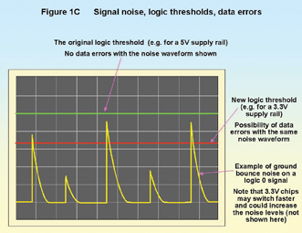
The higher levels and higher frequencies associated with these new and very desirable technologies cause problems for signal integrity, and the situation is made worse by the fact that these ICs typically operate on much less than 5V d.c. power (1.8V is not untypical) so their logic thresholds are lower and they are more vulnerable to interference.
Figure 1C shows an example of this issue causing a signal integrity problem, where acceptable noise levels in an existing design of PCB can result in unreliable digital operation if the ICs are replaced with otherwise identical equivalents that operate on a lower power supply voltage. Many designers have been surprised at how difficult it can be to simply convert an existing design to employ lower-voltage ICs.
The EMC techniques described in this series are often required for signal integrity reasons, just so that these types of ICs and IC packages can be made to function at all with any reliability.
To pass EMC compliance tests when these ICs are used may require all of the techniques described in this series plus shielding of the overall enclosure. However, the performance specifications for the enclosure-level shielding (and filtering) required will be much less, making the products less costly in manufacture, if these PCB EMC techniques are used in full.
1.5 Easier compliance for high-power DSP
Another situation that sometimes arises is very powerful digital signal processing, where numbers of ICs pass large quantities of data between themselves. The clock rates and signal edge speeds might not come within a decade of what is achieved in the core logic of a 130nm ‘system-on-a-chip’, but the relatively large distances the signals have to travel in their PCB traces can make their signal integrity difficult and their EMC compliance a significant challenge.
The PCB techniques described in this series help deal with both the signal integrity and EMC compliance of powerful DSPs in the easiest and lowest-cost manner.
1.6 Improving the immunity of analogue circuits
Analogue designers working with low frequencies (e.g. d.c. to 10MHz) might assume that all the fuss is about digital ICs and circuits and needn’t bother them. But all analogue semiconductors and ICs contain non-linearities (that is why they are called semiconductors, after all) and the small silicon feature sizes they use mean that they will happily demodulate and intermodulate RF ‘noises’ to frequencies well over 1GHz.
In the early 1990s the author tested a product that was little more than an LM324 on a small PCB for its immunity to RF under the EMC Directive’s generic immunity standard for the industrial environment, EN 50082-2:1995 (now replaced by EN 61000-6-2), and found that it gave much higher error voltages when subjected to 1GHz than it did when subjected to 500MHz. The author has tested many all-analogue products for immunity and they all showed significant problems up to several hundred MHz, until fixed by applying EMC remedial measures to their circuit design, PCBs and enclosures, basically as described in all six parts of [2].
Now that all analogue electronics exists in an environment that is very polluted with man-made electromagnetic noise up to at least 2.5GHz, whether that pollution comes from external devices such as cellphones, or internal devices such as switch-mode power converters or digital processing, PCB EMC techniques are now necessary to achieve their desired levels of immunity (and hence their signal-to-noise ratios) most easily and with the lowest cost.
2 What do we mean by “high speed”
‘High speed’ is hard to define exactly, but in the context of digital PCB design and layout it usually means signals with edge-rates that are so short that the dimensions of the PCB start to have a significant effect on the signal voltages and currents.
Another way to look at it is to say that the PCB dimensions are so large compared with the propagation time of the signal’s edge that the PCB’s traces and planes start to behave as resonant transmission lines instead of ‘lumped’ constants (e.g. milliohms, picofarads, nanohenries).
The velocity of electromagnetic propagation is limited by the laws of nature, and in an FR4 PCB it is approximately 50% of the free-space velocity of 3.108 m/s, say 6.67ns per metre (2ns per foot). So we can associate an ‘edge length’ in millimetres or inches with each rising or falling edge of a signal. So a 1ns edge has an ’edge length’ in an FR4 PCB of approximately 75mm (3 inches).
The rule of thumb is that we usually need to design the PCB using transmission-line techniques when the edge length is shorter than three times the longest dimension of a PCB. So for a PCB that has a longest dimension of 150mm (6 inches) we would categorise edge rates of 3ns and less as “high-speed”. Figure 1D shows this relationship.
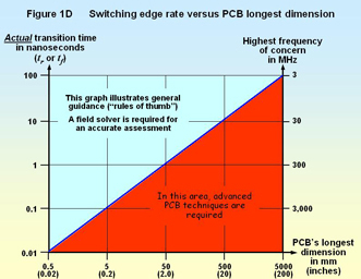
The above sounds quite straightforward – all we have to do is look in the devices’ data sheets for their rise and fall times to see whether we need to use advanced PCB techniques. But, as usual, real life is not so obliging – notice that figure 1D refers to the actual transition time. Rise and fall times may not even be given in the data sheets for some ICs, and in any case they only specify the maximum values. Actual transition times experienced in real life can be much less than what is specified on a data sheet, and will often be somewhere between a half and one-eighth. This allows the semiconductor manufacturers to shrink their silicon processes so as to squeeze more chips onto a wafer, improve yields, and make more money without the expense of updating their data sheets every time they do one of these ‘die shrinks’.
So a venerable glue logic device with a specified maximum rise and fall time of 6ns might nowadays be made on a silicon process that is ten times smaller than when it was first introduced to grateful designers, and might switch in under 1ns. Since some estimates have it that 30% of the USA’s gross national product depends on silicon feature sizes shrinking year-on-year in accordance with Moore’s law, for ever, we can see that it won’t be long before all devices are “high speed” and all PCBs need to be designed using advanced techniques that take full account of the transmission line behaviour of traces and planes.
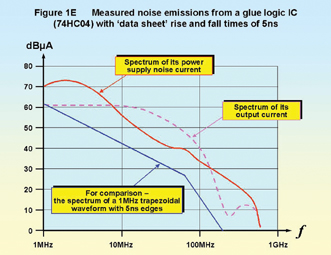
Figure 1E shows the measured noise emissions from a basic HCMOS glue logic IC, showing that it is generating frequencies on its outputs and power pins that go far beyond what would be expected from its data sheet specification.
Another issue is that many VLSI ICs have ‘core logic’ processes that use much smaller devices than their output drivers, and operate at much higher frequencies than the overall system clock, with much faster signal edges. These cause transient signals to be injected into the PCB’s 0V and power distribution systems, and common-mode noises on all the I/Os (often referred to as ‘ground bounce’ or ‘rail collapse’). The edge rates of these power transients and common-mode noises can be under 100 picoseconds, which we would categorise as “high speed “ for a PCB with longest dimension of only 5mm.
For analogue circuits, the “edge length is shorter than three times the longest dimension of a PCB” rule of thumb becomes the “tenth of the wavelength at the highest frequency of concern” rule, usually written as λ MIN/10 (since the minimum wavelength, λ , of concern is associated with the maximum frequency or concern).
Note that the wavelengths that matter are the ones that occur inside the PCB, and due to the slower velocity or propagation in a PCB (about 50% of the velocity in air) they are about 50% shorter than the wavelengths associated with the same frequency in air. So instead of the λ MIN/10 guide, some designers prefer to use a λ MIN/20 rule of thumb, where the wavelength is calculated as if the signal concerned was in air instead of in a PCB. The relationship between highest frequency of concern and PCB dimension is also shown in figure 1D.
3 Electronic trends, and their implications for PCBs
3.1 Shrinking silicon
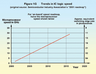
Section 2.1 above said that some estimates have it that 30% of the USA’s gross national product depends on silicon feature sizes shrinking year-on-year in accordance with Moore’s law, for ever. This trend is published as a an ‘official roadmap’ by the Semiconductor Industry Association, which is a major multinational organisation. Figures 1F and 1G are derived from the roadmap they published in 2001.
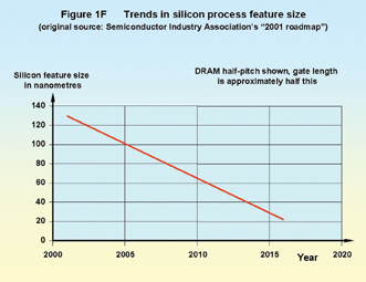
IC trends are driven by higher speed of operation, increasing complexity (more transistors per IC), improving wafer yield, and the cost to make each ‘chip’. All of these aims are what is driving the electronics industry to create more advanced products at lower costs, and even to address markets that were previously impossible, and they are all achieved by shrinking the feature sizes on the silicon wafer.
The established state of the art in silicon feature size is (at the time of writing) 0.13 microns (130nm) with a number of companies developing 90nm processes and research progressing on 65nm. Some semiconductor companies are already claiming to have 90nm or 65nm products in production, but these processes are not yet sufficiently well-developed to be in widespread use. There is an unstoppable trend towards smaller feature sizes and this is very good news for the future applications of electronic technologies.
But all this silicon high-technology has an inevitable downside for EMC and signal integrity. The EMC effects of shrinking feature size include…
- ICs that are more vulnerable to over-voltage damage (insulation layers are thinner)
- Data ‘bits’ are more vulnerable to data corruption (due to wider bandwidth and lower capacitance)
- Increasing emissions
The increasing emissions occurs because smaller silicon feature sizes means…
- less capacitance in the devices
- faster switching edges (shorter transition times)
- hence more energy in a harmonic spectrum that extends to higher frequencies
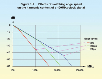
It is important to note that it is not the clock frequency that is important here – it is the switching transition time. Even if the clock frequency doesn’t increase, using smaller silicon processes increases the emissions significantly. Figure 1H shows the effects of changing the switching edge speed on the harmonics of a 100MHz clock.
The shrinking silicon feature size issue applies to all digital ICs including ‘glue logic’, not just VLSI and high-speed devices. It also applies to some analogue ICs. ICs are being made using silicon fabrication processes that employ ever-smaller feature sizes simply to improve the yield from the silicon wafers to make more money for the semiconductor companies.
So even buying the same old devices doesn’t protect a manufacturer from ‘die shrinks’, and a new batch of ICs can make a previously EMC-compliant product non-compliant, or even make its operation unreliable by compromising signal integrity. The needs of the semiconductor companies to earn more money for their shareholders has been known to cost some of their customers many millions of dollars in having to redesign their entire existing portfolio of products. Of course, while you are busy redesigning all your existing products, you have no resources to spare for designing new ones, and this can have the most serious financial implications for a manufacturing company.
3.2 Shrinking packaging
Smaller packages have lower inductances in their bond wires and lead frames, which can increase the levels of very high-speed core noise that ‘leaks out’ via the I/O and power/reference pins, and also allows the true ‘sharpness’ of an output driver’s transitions to be applied to the PCB’s conductors.
Designers have often been surprised at the signal integrity and EMC problems caused by simply replacing a device with the same type in a smaller package. One designer used a chip-scale IC in 2000, operating at the very low clock frequency of 1kHz, and was amazed to find that his product was failing emissions tests at 1GHz, due to the 1 millionth harmonic of the clock.
‘Chip-scale’ packages which are hardly any larger than the silicon chip itself are the ultimate expression of this packaging trend, and generally require the use of microvia PCB construction (see part 7 of this series). Chip-scale devices allow enormous improvements in miniaturisation, so there will be great pressure to use them.
Smaller packages can in fact help to improve EMC, but only if advanced PCB techniques are applied early in a project.
3.3 Shrinking supply voltages
To reach higher speeds (and reduce thermal dissipation) ICs and communications are using increasingly lower voltages, and the problems that the resulting lower logic threshold voltages can cause were briefly discussed in 1.4 above and Figure 1C.
Because of the ever-increasing numbers of semiconductors integrated in modern ICs, the amount of power required is increasing, so the supply voltages are continually decreasing to try to stop ICs from failing due to overtemperature, and (in battery-powered products) to extend battery life.
The result is that power supplies need a lower source impedance and a higher accuracy (tighter voltage tolerances). And since the IC loads operate at ever-higher frequencies they need their low source impedance to be maintained to ever-higher frequencies. Figure 1J shows an example of the trend that has occurred over the past few years.

The achievement of such low supply impedances (e.g. 0.4 milliOhms) at up to such high frequencies (e.g. 1200MHz) requires very advanced PCB design techniques, and these are discussed in parts 4 and 5 of this series. A great deal of noise is emitted by ICs into their d.c. supplies, as shown in figure 1E. At some frequencies the supply noise currents can be higher than the output currents, and as a result the ‘accidental antenna’ behaviour of the d.c. supply distribution on a PCB can sometimes contribute more to a PCB’s electromagnetic emissions than the actual signals. So d.c. supply impedance is an important EMC issue.
Of course the trend shown in figure 1J is continuing, although there seems little possibility in decreasing the supply voltage below, say, 0.8V due to the silicon band-gap voltage being around 0.6V. Increased power requires higher efficiency and more sophisticated cooling techniques are needed, and with the higher frequencies being used the heat-removal devices (e.g. heatsinks, heat pipes, etc.) now need to be designed for EMC too, so that they do not behave as resonant structures (accidental antennas).
3.4 PCBs are becoming as important as hardware and software
To cope with IC trends, the typical PCB of the future will be a very high-technology component indeed. It will be a network of microwave transmission lines, not simply a convenient way to interconnect devices (no longer simply a ‘printed wiring board’) – and it will need to be designed in parallel with a sophisticated cooling system.
At the time of writing, more than 50% of the volume of global PCB manufacture uses 6 - 12 layers, and 4 layers or less are only used for the simplest circuits. More than 50% of the volume of global PCB manufacture is also “controlled-impedance” using transmission-line design techniques.
PCB design and layout is becoming just as vital to the product’s function as all of the hardware and all of the software. PCB designers may once have been little more than draughtsmen, but increasingly they are having to actually design their PCBs according to electrical specifications, as described later, and need an understanding of wave propagation and the ability to drive sophisticated field solvers.
3.5 EMC testing trends
The FCC in the USA already require testing of emissions at 5 times the highest clock frequency, or 40GHz, whichever is the lower. And the latest draft of IEC 61000-4-3 which describes basic immunity testing method for radiated RF fields will cover up to 6GHz.
There is no sign of any end to this trend, because the radio spectrum between 1 and 60GHz is increasingly being used for communications and so needs protecting from ‘unintentional transmitters’. High-volume low-cost motor cars are just beginning to be fitted with anti-collision systems that fit each vehicle with a radar operating at 77GHz. The future for electronics design and manufacture is very exciting, but EMC is going to become a truly major headache.
4 Managing designing to reduce timescale risk and warranty costs
4.1 Guidelines, maths formulae, and field solvers
The difficulty of designing PCBs so that circuits will function at all, let alone meet EMC requirements, is increasing at a much faster rate than silicon processes are shrinking and clock speeds increasing. But we need to reduce time-to-market, not increase it, so we need to use methods of designing PCBs so that they achieve functionality and EMC without time-consuming iterations, preferably without any iterations at all – ‘correct by design’. Two design methodologies help here: virtual design; and experimental verification.
Desirable skills for PCB designers, just to cope with modern signal integrity problems in high-speed PCBs (see 2 above), never mind EMC, which is harder, include familiarity with both 2-D and 3-D field solvers (which now run on PCs), and the ability to design PCBs to meet electrical specifications such as…
- skew limits
- maximum crosstalk (% or dB) for each trace
- maximum inductances for some traces
- minimum rise/fall times, etc., etc.
There will need to be some iteration between PCB layout and circuit design (e.g. terminating traces which are found to need to be transmission lines due to their length) – to save having to iterate the design of the physical PCB when it is found to suffer signal integrity and/or EMC problems later in the project (see figure 1A for the cost benefits of fixing problems early in the design and development cycle).
General guides (“rules of thumb”) such as those given in [1] - [4] and this series of articles should be used from the very first to estimate orders of magnitude, and used throughout a project to ‘sanity check’ calculations and the outputs of computer-based simulators.
All practical mathematical formulae that can be used by a practising design engineer are based on simplifications and assumptions that result in inaccuracies, and may not even be true in some instances. As a result they are only appropriate for analytical approximations, quick estimates, and early design tradeoffs. However, it is getting easier to use field solver and circuit simulator software packages running on PCs instead of hand-cranked sums.
Field solvers are the only method that will confirm the signal integrity of an actual design before it is constructed and tested for the first time. Field solvers are getting better and costing less all the time, so one day we will be able to simulate the EMC of our completed designs – but we are still some way from that desirable situation at the time of writing.
4.2 Virtual design
It was mentioned earlier that some electronics industries have very short product lifetimes. These include PC motherboards, PC hard disc drives, PC graphics cards, cellphones, etc., and they often use ICs that have only just been released and for which no experience has been gained. With product lifetimes of 90 days or so, such companies must be confident that they can avoid PCB iterations that would cause them to be late to market. They use virtual design techniques based on circuit simulators and field solvers which interact so as to allow numerous design iterations that prove the PCB layout before the first PCB is even photoplotted.
Circuit simulators come in two main flavours: IBIS [5] and SPICE. It is claimed that IBIS handles complexity more easily than SPICE, and that more IBIS models exist. It is also easier and quicker to generate an IBIS model for a new IC.
Field solvers include 2-dimensional and 3-dimensional types based on a variety of modelling techniques, such as…
- FDTD (Finite Difference Time Domain)
- FEM (Finite Element Model)
- TL (Transmission Line)
- MOM (Method of Moments)
To reduce calculation time to what is achievable with today’s computers (including supercomputers) field solvers use a form of finite element analysis. They divide the structure to be simulated into very small cells, which must be much smaller than the shortest wavelength that can be created by the devices and circuit. They then solve simplified versions of Maxwell’s equations for each small cell in turn. Fields solvers can be used to optimise precise trace widths, dielectric thicknesses, and board stack-up for a target characteristic impedance, determine crosstalk, ground bounce and rail collapse, and many other signal integrity specifications. Some solvers also have limited EMC analysis tools.
There are also field solvers that are aimed at solving EMC problems rather than signal integrity (e.g.[6]) but at the time of writing they are limited to ‘what if’ investigations on simplified versions of the final design, and cannot be integrated with the virtual design flow described below.
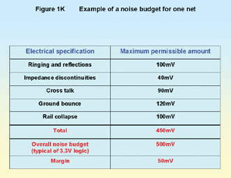
In a virtual design and test methodology the circuit is first simulated using IBIS or SPICE, using appropriate models for the active and passive devices, including any wires and connectors. When the circuit simulates correctly, automatic netlisting sends a ‘rats nest’ to the PCB designer’s software application to prevents logical errors in PCB layout. The circuit designer will have a noise budget for each net (Figure 1K shows an example noise budget) and will communicate the following electrical requirements to the PCB designer...
- Segregation issues and critical component placement, shielding cans, etc. (see part 2 of this series)
- Characteristic impedances for some or all nets.
- Maximum values for ringing and reflections for each net
- Maximum values of impedance discontinuities for some or all nets
- Maximum values of cross talk for each net
- Maximum values of ground bounce for each net
- Maximum values of rail collapse for each net
- Flight times for some or all nets
- Maximum inductances for power supply decoupler traces
- Skew limits between nets
The PCB designer performs ‘what if’ simulations on critical parts of PCB’s physical structure (trace width, stack-up, etc.) using the appropriate in 2-D or 3-D field solvers, using appropriate parameters for final manufacture (e.g. PCB dielectric constant, copper lossiness, etc.), to meet the electrical design criteria for the PCB, and comes up with a first pass at the layout.
The field solver then automatically extracts the draft PCB layout’s parasitics (partial and mutual inductances, stray capacitances, flight times, etc.,) and sends them to the circuit simulator. The circuit simulator adds the PCB’s electrical characteristics to the circuit the designer captured, and re-simulates it to see if it still functions within specification. The designer then makes the appropriate modifications, where necessary, to make the circuit simulate correctly again.
The PCB’s electrical characteristics are an important part of the ‘hidden schematic’, which also includes the complex behaviour of the active and passive devices at high frequencies (which should have already been entered in to the circuit simulator). The hidden schematic for even a simple circuit is at least an order of magnitude more complex than the circuit that is drawn on a typical schematic or circuit diagram. For a complex circuit it can be two orders of magnitude larger.
When a PCB electrical parameter is out of specification, there are often a great many possible contributors. The task of discovering which ones to vary to achieve the specification can seem daunting, but ‘sensitivity analysis’ comes to the designer’s rescue. Circuit simulators and field solvers permit complex ‘what if’ investigations, and these can be used to discover the sensitivity of the chosen parameter (e.g. overshoot height, trace impedance, crosstalk, decoupling inductance) to the various physical design issues. Sensitivity analyses helps to avoid wasting time over insignificant issues, setting overly tough PCB fabrication tolerances, or having to do multiple ‘trace tuning’ PCB iterations.
The virtual design is iterated between the circuit simulator and the PCB field solver until both designers are happy with the result. This iterative process usually only applies the field solver to the critical areas, because at the time of writing it takes too long to run a full solver analysis on a typical PCB. But before the PCB’s layout is released for its first prototype manufacture it is fully simulated in the field solver and all of its parasitics fed back to the circuit simulator to prove that the circuit still simulates correctly. Now the first prototype of the PCB is virtually guaranteed to have no errors and to function correctly without signal integrity problems, for nominal specification components.
Of course, devices with nominal specifications hardly ever occur, and all device parameters vary with temperature (e.g. switching rise and fall times are shorter at lower temperatures). So to prove that the design will give an acceptable yield in volume manufacture, and be reliable enough when exposed to temperature variations in real life operation – the circuit simulator performs Monte-Carlo analysis or parametric sweeps on the components’ tolerances, plus temperature analyses on the components’ temperature coefficients, on the final design. Figure 1L shows an example of a virtual PCB design project flow.

The virtual design process as described above can really only ensure signal integrity and assist the achievement of reliability and lower warranty costs (at the time of writing). It cannot (yet) be used to ensure EMC compliance. But because high-frequency signal integrity issues are also EMC issues, it is possible to use this methodology to help ensure adequate EMC performance.
There is, of course, a learning curve associated with these circuit simulators and field solvers, and of course there is the business of developing a model library that includes not only the 3-dimensional attributes but also all the high-frequency behaviour of the components, the tolerances of their various parameters, and their temperature coefficients. And, of course, suppliers can be late delivering the latest version and there can be bugs in the software, and nothing ever goes as smoothly as we would like (Murphy’s Law applies to all human endeavours). So, if it intended to use virtual design on a new project, sufficient time must be allowed for the acquisition of the software, development of the models and training of the staff, and to allow for the normal operation of Murphy’s Law.
Virtual design as described above is now possible with relatively easy-to-use packages that run on a modern PC. Of course, they are not cheap, but they are very reasonable when compared with the true cost of even a single iteration of all the schematics and PCBs on a single product, especially if that design iteration could occur at a late stage in a project. Compared with the true cost of being late to market, most companies could afford the very best simulators and field solvers, high-power workstations to run them on, and training courses for the staff that will use them.
4.3 Experimental verification
Models are never 100% accurate, and they don’t model everything. Simulators are never 100% accurate and the assumptions they have made in order to achieve reasonable computation times might not be appropriate in all circumstances. And of course virtual design methodology cannot yet be fully applied to EMC due to the complexity involved in simulating the EMC of a real PCB with its cables and enclosure.
Considering figure 1A, we can see that we really must not leave any technical risks beyond a certain point in a project – so experimental verification is recommended for all risky design issues (which we might call potential “show-stoppers”). The risky circuit areas and their PCB layouts should be physically created and tested, as early in a project as possible.
Ideally, impedance analysers, network analysers, and time domain reflectometers would be used to prove the design of the risky area, and some very commercial companies are equipped with many hundreds of thousands of dollars worth of such equipment, plus sophisticated probing devices that can operate to many GHz, just for this purpose.
But even if the only equipment that is available is fast oscilloscopes (with suitable high-frequency probing techniques), bit error rate testers, and other equipment likely to be found in the typical electronics company, quite a lot of useful de-risking information can be obtained from an experimental PCB. Specialist instruments such as network analysers can be hired, but getting useful results from them may require a learning curve.
To improve reliability in the field, experimental circuits can be tested with forced cooling and heating of the experimental PCB. To improve yields in volume production is more difficult, as a wide variety of components with different tolerances are usually not available, and if they were, substituting them would take too long. But testing experimental circuits whilst cooling and heating individual devices considerably beyond their anticipated ambient range (e.g. from -40 to +120 degrees Celsius, taking care to avoid damage to scarce samples) will vary some of their parameters over a wide range and can help achieve a good yield in volume production.
5 References
[1] “Design Techniques for EMC – Part 5: PCB Design and Layout”, Keith Armstrong, UK EMC Journal, October 1999, pages 5 - 17
[2] “Design Techniques for EMC – Part 5: PCB Design and Layout”, Keith Armstrong, http://www.compliance-club.com/KeithArmstrongPortfolio
[3] “PCB Design Techniques for Lowest-Cost EMC Compliance: Part 1” M K Armstrong, IEE Electronics and Communication Engineering Journal, Vol. 11 No. 4 August 1999, pages 185-194
[4] “PCB Design Techniques for Lowest-Cost EMC Compliance: Part 2” M K Armstrong, IEE Electronics and Communication Engineering Journal, Vol. 11 No. 5 October 1999, pages 219-226
[5] The Official IBIS Website: http://www.eigroup.org/ibis/ibis.htm
[6] Flo-EMC from Flomerics Ltd, http://www.flomerics.com Ansoft, http://www.ansoft.com/
I would like to reference all of the academic studies that back-up the practical techniques described in this series, but the reference list would take longer to write than the series! But I must mention the papers presented at the annual IEEE International EMC Symposia organised by the IEEE’s EMC Society (http://www.ewh.ieee.org/soc/emcs), especially the dozens of wonderful papers by Todd Hubing’s staff and students at the University of Missoura-Rolla EMC Lab (http://www.emclab.umr.edu), and papers by Bruce Archambeault of IBM and the EMC experts at Sun Microsystems.
Many other contributors to the IEEE EMC Symposia, and other conferences and symposia and private correspondence are far too numerous to be named in a magazine article like this, but the following names stand out: Tim Williams of Elmac Services, http://www.elmac.co.uk; Mark Montrose of Montrose Compliance Services, http://www.montrosecompliance.com; John Howard, http://www.emcguru.com; Tim Jarvis of RadioCAD, http://www.radiocad.com; Eric Bogatin of Giga-Test Labs, http://www.gigatest.com; and dozens of application notes from National Semiconductor; Rambus Corp.; California Micro Devices; Intel; IBM; Cypress Semiconductor; Xilinx; Sun; Motorola; AVX; X2Y Attenuators; Giga-Test Labs; Ansoft and Flomerics. I apologise to all of the excellent people and companies that I have left out.
Some useful textbooks and other references are:
[A] “EMC and the Printed Circuit Board, design, theory, and layout made simple”, Mark I. Montrose, IEEE Press, 1999, ISBN 0-7803-4703-X
[B] “Printed Circuit Board Design Techniques for EMC Compliance, Second Edition”, Mark I. Montrose, IEEE Press, 2000, ISBN 0-7803-5376-5
[C] “High Speed Digital Design, a Handbook of Black Magic”, Howard W Johnson and M Graham, Prentice Hall, 1993, ISBN 0-1339-5724-1
[D] “High Speed Signal Propagation: Advanced Black Magic” Howard W. Johnson, Prentice Hall, 2003, ISBN: 0-1308-4408-X
Eur Ing Keith Armstrong C.Eng MIEE MIEEE
Cherry Clough Consultants, Member of: EMCTLA, EMCUK, EMCIA
HYPERLINK "mailto:keith.armstrong@cherryclough.com" keith.armstrong@cherryclough.com