This is the sixth in a series of eight articles on good-practice design techniques for electromagnetic compatibility (EMC) for printed circuit board (PCB) design and layout. This series is intended for the designers of any electronic circuits that are to be constructed on PCBs, and of course for the PCB designers themselves. All applications areas are covered, from household appliances; commercial, medical and industrial equipment; through automotive, rail and marine to aerospace and military.
- Saving time and cost overall
- Segregation and interface suppression
- PCB-chassis bonding
- Reference planes for 0V and power
- Decoupling, including buried capacitance technology
- Transmission lines
- Routing and layer stacking, including microvia technology
- A number of miscellaneous final issues
A previous series by the same author in the EMC & Compliance Journal in 1999 “Design Techniques for EMC” [1] included a section on PCB design and layout (“Part 5 – PCB Design and Layout”, October 1999, pages 5 – 17), but only set out to cover the most basic PCB techniques for EMC – the ones that all PCBs should follow no matter how simple their circuits. That series is posted on the web and the web versions have been substantially improved over the intervening years [2]. Other articles and publications by this author (e.g. [3] [4] and Volume 3 of [5]) have also addressed basic PCB techniques for EMC.
Like the above articles, this series will not spend much time analysing why these techniques work, it will focus on describing their practical applications and when they are appropriate. But these techniques are well-proven in practice by numerous designers world-wide, and the reasons why they work are understood by academics, so they can be used with confidence. There are few techniques described in this series that are relatively unproven, and this will be mentioned where appropriate.
Table of Contents, for this Part of the series
Section 1 is contained in Issue 57, March 2005
1 Matched transmission lines on PCBs
1.1 Introduction
1.2 Propagation velocity, V and characteristic impedance, Z0
1.3 The effects of impedance discontinuities
1.4 The effects of keeping Z0 constant
1.5 Time Domain Reflectometry (TDR)
1.6 When to use matched transmission lines
1.7 Increasing importance of matched transmission lines for modern products
1.8 It is the real rise/fall times that matter
1.9 Noises and immunity should also be taken into account
1.10 Calculating the waveforms at each end of a trace
1.11 Examples of two common types of transmission lines
1.12 Coplanar transmission lines
1.13 The effects of capacitive loading
1.14 The need for PCB test traces
1.15 The relationship between rise time and frequency
Section 2 and 3 are contained in Issue 58, May 2005
2 Terminating transmission lines
2.1 A range of termination methods
2.2 Difficulties with drivers
2.3 Compromises in line matching
2.4 ICs with ‘smart’ terminators
2.5 Bi-directional terminations
2.6 Non-linear termination techniques
2.7 ‘Equalising’ terminations
3 Transmission line routing constraints
3.1 General routing guidelines
3.2 A transmission line exiting a product via a cable
3.3 Interconnections between PCBs inside a product
3.4 Changing plane layers within one PCB
3.5 Crossing plane breaks or gaps within one PCB
3.6 Avoid sharp corners in traces
3.7 Linking return current planes with vias or decaps
3.8 Effects of via stubs
3.9 Effects of routing around via fields
3.10 Other effects of the PCB stack-up and routing
3.11 Some issues with microstrip
In this Issue:
4 Differential matched transmission lines
4.1 Introduction to differential signalling
4.2 CM and DM characteristic impedances in differential lines
4.3 Exiting PCBs, or crossing plane splits with differential lines
4.4 Controlling imbalance in differential signalling
4.5 Routing asymmetry
5 Choosing a dielectric
5.1 Effects of woven substrates (like FR4 and G-10)
5.2 Other types of PCB dielectrics
6 Matched-impedance connectors
7 Shielded PCB transmission lines
7.1 ‘Channelised’ striplines
7.2 Creating fully shielded transmission lines inside a PCB
8 Miscellaneous related issues
8.1 Impedance matching, transforming and AC coupling
8.2 A ‘safety margin’ is a good idea
8.3 Filtering
8.4 CM chokes
8.5 Replacing parallel busses with serial
8.6 The lossiness of FR4 and copper
8.7 Problems with coated microstrip
8.8 The effects of bond-wires and leads
9 Simulators and solvers help design matched transmission lines
10 EMC-competent QA, change control, cost-reduction
11 Compromises
12 References
13 Some useful sources of further information on PCB transmission lines
4 Differential matched transmission lines
4.1 Introduction to differential signalling
All the above has assumed signals use ‘single-ended signalling’ – that is: they are all generated and received with respect to 0V (sometimes with respect to some other voltage reference instead). But differential signalling is increasingly required for clocks and communications (e.g. USB2.0, Firewire, Ethernet, PCI Express [26]) for SI and EMC reasons. LVDS (low voltage differential signalling) technology is becoming increasingly commonplace, and PCI Express LVDS drivers have rise/fall times around 100ps.
Differential signalling uses two conductors driven in antiphase with each other. The result of a well-realised differential interconnection is better SI, lower emissions, increased immunity, and the creation of lower levels of ground and rail bounce noise.
Strictly speaking, and in an ideal world, there would be no need for any electrical connection between the reference voltages for the driver and receiver (but in the real world such connections help reduce common-mode emissions caused by imbalances, see later). Figure 6Y shows two examples of differential signalling. The first one is typical of digital differential signalling, which uses two single-ended signals with one of them being an inverted version of the other. Sometimes + and – symbols are appended to the signal name to indicate a differential pair, instead of using a bar above one of them. Other names for differential signalling include ‘symmetrical’ and ‘balanced’.

Digital devices and operational amplifiers can only handle signals within a certain voltage range, limited by their power supply rails. Making the differential signals referenced to 0V ensures that the signals remain within the optimum range for the devices, and the common 0V reference plane connection provides a nearby return path for common-mode currents caused by the imbalances in any real-life differential signalling scheme. Imbalances and the common-mode noises they create are discussed later.
Where signals start or end as single-ended, we need devices that convert them into differential signals, and back again, somewhere in our circuits. But many transducers, such as moving-coil microphones, platinum resistance thermometers and dipole antennas, actually generate differential signals directly. Digital and analogue ICs that employ differential signalling can include the single-ended to differential (and vice-versa) converter circuitry within themselves. Another technique, shown in Figure 6Y, is to use a transformer to covert from one mode to the other (see the section on line matching, later).
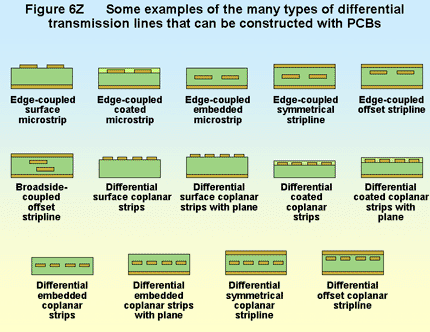
When the propagation delay along a differential conductor exceeds half the rise time of the signal (tp ≥ tr/2) a differential transmission line is required for SI and EMC, just as it is for the signals discussed in the previous sections. As before, some more conservative designers prefer to use (tp ≥ tr/3) and the author recommends (tp ≥ tr/8) for improved EMC. A wide variety of differential lines can be constructed on or in PCBs, as shown by Figure 6Z.
All of the discussions in the earlier sections on transmission lines for single-ended signals apply equally well for differential lines – but to obtain all the benefits of differential lines there are a number of additional considerations, and these are covered below.
4.2 CM and DM characteristic impedances in differential lines
The Z0 of each trace in a differential line depends on how each trace is driven with respect to the other. The even-mode Z0 (sometimes called the common-mode or CM Z0) of a differential line applies when both lines are driven in phase with each other. This is different from the odd-mode Z0 (sometimes called the differential-mode, or DM Z0) when both lines are driven in antiphase to each other. Yet another type of Z0 arises when one trace in each pair is driven on its own, with the other held static. [11] gives an example of designing, simulating and measuring differential lines in a backplane-based product, including TDR simulations and measurements of the actual even and odd mode impedance achieved in practice.
So differential Z0 only exists for differential-mode (DM) signals – but in real life no signals are ever perfectly balanced, and imperfections in the traces themselves also disturb their balance and give rise to common-mode (CM) voltages and currents. Unavoidable noises on traces, such as ground bounce and rail bounce, are also usually CM. So there are always CM signals and noises on differential transmission lines. Even when the DM Z0 is perfectly controlled along the traces, and perfectly matched by the resistors at the ends, the CM Z0 (which has a different value) also needs to be controlled and terminated. If the CM Z0 is not controlled along the trace to minimise impedance discontinuities, and if both traces are not terminated correctly by the resistors at their end(s), CM voltages and currents will be reflected – distorting both signal waveforms and possibly causing SI problems, but much more likely to cause significant EMC problems.
Until a few years ago the numerical formulae for calculating the various Z0s associated with differential transmission lines were disputed. There now appears to be good agreement between the various calculation methods and field solvers – but when using formulae make sure they are taken from documents that were written after 2000, or use software applications that have issue dates of 2000 or later. Anyway, it is best to use a field solver to calculate differential line Z0s (see later).
When routing traces carrying different signals on a PCB, they should be spaced far enough apart that their ‘stray’ capacitive and inductive coupling doesn’t cause crosstalk problems for SI (not discussed further here). But when routing a differential pair of signals they should be spaced as close together as is practical, to maximise the coupling between their traces. Such ‘closely coupled’ differential transmission line traces provide the best performance for both SI and EMC.
A differential transmission line that (for example) consists of two 50Ω transmission line traces that are so far apart that there is very little coupling between them, has a DM Z0 of 100Ω and a CM Z0 of 50Ω But when the lines are close enough to couple with each other, their DM Z0 decreases (e.g. to 67Ω) while their CM Z0 remains unchanged.
So always minimise the spacing between the traces to maximise their mutual inductance and the capacitance between them. And control the geometry of the trace pair along its entire route to minimise impedance discontinuities in the DM and CM Z0s. This helps to minimise imbalances in the differential line (see later) and is very important for EMC. When routing a section of a differential line on one PCB layer against a solid reference plane (or planes) this almost always requires that the traces’ widths and spacing remains constant along the section. (Ideally the whole length of a differential line would be one such section.) For a lot more information on routing differential transmission lines see [27], [28] and [29].
Figure 6AA shows some examples of terminating differential lines when using incident wave switching (see earlier, and Figure 6M). Using the above example, the resistors (R1A and B) from the traces to 0V would each be 50Ω, and the differential resistor (R2) would be 200Ω. The CM Z0 of 50Ω and is matched by R1A and B, whereas the DM Z0 of 67Ω is matched by R1A in series with R1B (100Ω), in parallel with R2.
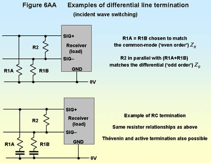
When using reflected wave switching (see earlier, and Figure 6L), both of the traces must be fitted with series resistors very close to the pins of their drivers. But it is impossible to match both the CM and DM characteristic impedances of closely-coupled transmission lines with just these two serial resistors. Another resistor will be required, connected between the two traces, to match the DM Z0, just as is required when terminating closely-coupled incident-wave switching differential transmission lines, as in the above example.
It is common to see differential transmission lines terminated with a single resistor between the two lines at the receiver, but this is only acceptable for EMC where CM chokes or other methods have been used to reduce the flow of common-mode (imbalance) current (see later) to negligible amounts.
It is also common to see differential lines terminated as if they were two independent single-ended lines, using series or shunt techniques. But this is only acceptable for EMC when the lines are so far apart that the coupling between them is negligible – and this is usually not the best type of routing for EMC anyway (although it may be the best possible when routing through a via field that does not permit two traces between pads, see later).
The important thing to remember where EMC is concerned, is that differential lines need to have all of their Z0’s terminated in matched resistors one or both ends, so that problems are not caused by reflections in either their DM or CM signals.
Differential traces can be routed coplanar, on the same PCB layer or broadside, on adjacent PCB layers. Broadside traces are generally poorer for SI and EMC, for a variety of reasons (see “Asymmetry in Broadside Configuration” in [12]) so are not generally preferred. However, the broadside configuration can sometimes help achieve the least-worst EMC, see later.
4.3 Exiting PCBs, or crossing plane splits with differential lines
Closely-coupled differential transmission lines are the best type of transmission line to use if a signal has to leave its reference plane – for example when exiting a board to leave a product; when connecting to a different board in the same product, or when a signal must become referred to a different reference plane in the same PCB. They are also the best types of transmission lines to use when a split or gap in the same reference plane has to be crossed – with coplanar differential lines being the very best for this. But the routing guidelines listed earlier should always be applied as far as is practical: differential lines are not a universal panacea. (Note that splits in planes are no longer generally recommended, either for SI or EMC, despite what semiconductor manufacturers’ application notes or older textbooks might recommend [20].)
Where a differential line must exit its reference plane, whether to exit a product via a cable, or to connect to another board, filtering may be needed at the point where it leaves its plane, just as was described above for single-ended lines. X2Y Attenuators LLC (http://www.x2y.com) have recently developed a new type of capacitor that is very suitable for filtering differential signals or power. It has three electrodes arranged symmetrically, with the centre electrode being the reference plane connection. [16] described using such capacitors for PCB decoupling, where their reduced self-inductance makes them effective at much higher frequencies than normal discrete decaps, but they behave even more like ideal capacitors when used with balanced signals (or power). Figure 6AB shows an example PCB layout using the X2Y® devices.

4.4 Controlling imbalance in differential signalling
To maximise the benefits of differential lines for SI and EMC, it is important to maintain their ‘balance’ along their entire routes. Some guidance on this is given in [29], and in [26] (for PCI Express). Where planes suffer from gaps, or where shielded cables do not use true 360° termination at both ends, just 150ps of skew between the + and – signals can degrade the EMC performance of a differential line so that it is no better than using a single single-ended trace instead. There are numerous possible causes for differential signal skew, and these are the subjects of this sub-section.
The reason for this degraded EMC performance is shown in Figure 6AC. Line imbalance causes the relative timing (skew) of the differential signals to worsen, which directly results in CM currents. These must flow in a common connection between the driver and the load, usually the common reference plane. Where this common connection isn’t very low impedance at the highest frequency of concern and where it is not in intimate physical proximity with the differential traces (or connectors or other conductors) along their entire route: just 150ps of skew causes DM to CM conversion (and vice-versa) that can cause problems for emissions (and immunity).
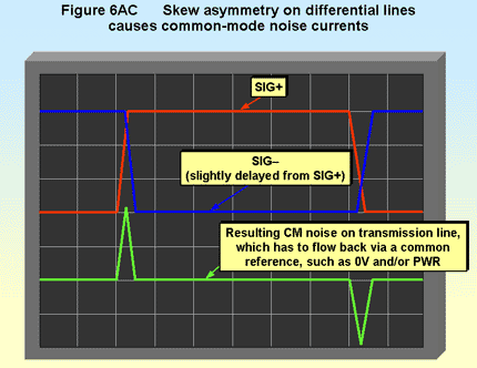
The CM voltage associated with a differential signal is related directly to the skew – a differential skew of X% of a signal’s rise/falltime results in a CM voltage that is X/2% of the differential signal voltage (see “Common Mode Analysis of Skew” in [12]).
There are a number of sources of imbalance that can affect the differential skew and hence compromise the emissions and immunity, including…
- Unequal stray coupling to the traces (e.g. one line is closer to the edge of the PCB, or to a gap or edge in the reference plane, or closer to a metal object, than the other; variations in trace spacing).
- Differences in trace widths.
- Propagation time differences for the + and – signals, caused by line length differences between the two traces; and/or differences in their propagation velocity.
- Driver timing asymmetry.
- Different driver impedances, pull-up to pull-down.
Each of these contributions is discussed in more detail below. It is recommended that a ‘differential skew budget’ is set, and the contributions from all of these different issues assessed to ensure that the majority of the PCBs will not have EMC problems due to this cause.
But following all the EMC guidance in this article, for example: routing using striplines on only one PCB layer, with uninterrupted reference planes that extend well beyond the traces on all four sides, would make differential skew less of an EMC problem. It is rare that designs are completed without some compromises somewhere, so field solver simulations (see later) may be required to discover just what the differential skew budget should be for a given interconnection.
Unequal stray coupling to the traces
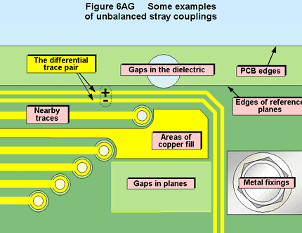
When differential traces pass near metal, plastic, epoxy, ceramic or glass objects; plane gaps and edges; other traces; mounting screws, etc, one trace will have different ‘strays’ than the other, and the resulting line imbalance causes emissions to increase (because more of the wanted DM signal is converted into unwanted CM noise). Figure 6AG shows some typical examples of this.
Keep each trace well away from edges, gaps or holes in any planes, and any large vias or metal fixings. Ideally keep both traces more than D/10 away from the edge of a plane of dimension D. Recommended layouts for such situations can be found in application notes, articles and papers, (for example, the guidance on “avoiding differential pair routing violations” in [29]) – but most of these are only concerned with what is acceptable for SI. Good line balance for good EMC is much harder to achieve than acceptable SI, but (as mentioned at the beginning) setting tougher SI specifications than are necessary just for SI will generally help achieve better EMC.
Choose connector pins that have identical stray capacitance and pin length, which usually means they are symmetrical with respect to the shell and the other pins. Tests have shown that using the wrong pins for a differential line in a 15-way shielded D-type can increase emissions by 20dB.
Using stripline routing can help maintain differential line balance. Stripline between two unbroken planes is best, with vias or decaps linking the two planes at least every λ/10 over the whole PCB (at the highest frequency of concern), because the two traces are better ‘shielded’ from stray external capacitance and mutual inductance, and this reduces the unbalancing influence of lumps of metal or dielectric that are mounted on or near to the PCB.
Keep the differential line’s trace spacing constant, and try (wherever possible) not to split them when passing vias or other gaps in their traces’ reference plane. Avoid splitting differential traces as they pass through a field of vias such as under a BGA IC or a dense multiway connector – this often means using smaller ‘track and space’ layout widths than are offered by the lowest-cost PCB manufacturers [30]. Alternatively, use microvia/HDI PCB techniques instead of THP – discussed in more detail in Part 7 of this series.
Difference in trace widths
Variations in trace width during PCB fabrication can be a cause of imbalance. These can be caused by variations in the rate of copper foil etching, and/or variations in any subsequent plating, over the length or width of the PCB. Errors in trace width and spacing can also occur, depending on where they land on the virtual grid produced by the natural resolution of the Gerber phototool [31].
For single-ended transmission lines the effect of erroneous trace widths caused by the above is usually only considered to be significant when trace widths that are less than 0.13 mm (5 thou). But for differential lines, the effect on line balance (and therefore on DM-CM conversion and hence emissions) can be significant. To control process variations it is important to include test coupons at two or more widely-separated locations on a PCB, so that manufacturing quality can be checked at the Goods Receiving department as part of a goods acceptance procedure [15].
It is quite possible that PCB test coupons would not detect trace width errors caused by the Gerber resolution, so the usual way of overcoming this problem (without using non-woven dielectrics, see below) is to route all narrow differential lines at angles of between 20° and 70° to the grid of the Gerber digitiser, so any effects due to digitisation cancels out sufficiently well on average along the traces.
Testing differential line test coupons requires the use of a 4-port vector network analyser, which used to be a very specialist and expensive piece of scientific equipment, but versions are now available suitable for testing at Goods Receiving, from manufacturers such as Polar Instruments [14].
Propagation time differences for the + and – signals
Where the signal route includes connectors and/or cables, note that 150ps of skew (see above) can be caused by about 20mm of path length difference in a stripline PCB trace in FR4, or 30 to 40mm of path length difference in a connector or cable (depending on their dielectrics). So, where reference planes or cable shields are not perfect along an entire route, to obtain significant EMC benefits from differential signalling when path length differences are the sole cause of differential signal skew – we should aim for path length differences to be no more than one-tenth of these figures. But there are other contributions to skew too, so we probably need to aim for path length differences that are one-twentieth of the above figures, or less.
Differences in their propagation velocity V between the two traces can be caused by trace routing on woven glass-epoxy substrates (such as FR4 and G-10). This has the same effect as a difference in the trace lengths. Routing differential lines at an angle of between 30° and 60° to the warp or weft of the fibreglass layers is usually enough to ‘average out’ the effects of the woven substrate [32] [33]. This issue is discussed in more detail in a later section.
Driver timing asymmetry (between + and – signals)
Better driver timing symmetry means that the + and – signals switch more nearly at the same instant (or in the case of sinewave signals, have less phase difference). The result is lower differential skew, which in turn means lower CM emissions from this cause.
So always check data sheets for maximum differential skew data. If it isn’t in the data sheet, assume the specification is too poor. Even if a device measures correctly in a test rig, the manufacturer may at some point in the future ship devices that explore the entire ‘specification space’ permitted by his data sheet (see Chapter 15 of [34]) – so unless the maximum specification in the data sheet (or in a letter from the manufacturer) is good enough for a design, choose a device with a better specification.
For example, the data sheet for the DC90C031 LVDS Quad CMOS Differential Line Driver specifies its typical rise/fall time as 350ns and its differential skew as 80ps typical but 900ps maximum. Clearly, when using such a device, attention to the detail of the CM current return path is going to be important for good EMC performance from the PCB and the lowest cost products.
Different driver impedances, pull-up to pull-down (driver output asymmetry)
Unequal output impedances between pulling up and pulling down can make square waves rectangular. A real-life CMOS driver example has an output impedance of 44Ω when pulling up, but 11Ω when pulling down. Since the transmission line has a real impedance (typically somewhere between 50 and 120Ω), the result (in this example) is that the positive-going transitions propagate with different timing from the negative-going transitions.
Where the signal was intended to be a squarewave clock, the result is a rectangular wave and one effect of this is emissions at even-order harmonics of the clock frequency. (A pure squarewave only has odd-order harmonics in its Fourier spectrum.) But for differential lines it contributes to driver skew asymmetry, increasing CM noise emissions.
Adding some series resistance at the driver end of the transmission line can help a little. For example, adding 22Ω at the output of the driver should – in the above example – reduce even-order emissions by around 6dB. However, it is much more effective to use devices containing drivers that are designed for driving transmission lines. These will usually have a low impedance (e.g. 10Ω) when pulling up or down, but always check the data sheet (or ask the manufacturer) for the worst-case difference between the pull-up and pull-down impedance, and use the devices for which the specifications prove they will be good enough in the actual PCB, taking all the other sources of differential skew into account.
4.5 Routing asymmetry
The importance of symmetrical routing of the traces in a differential pair was mentioned earlier, and of course routing the lines differently will alter the stray capacitances and inductances each is subject to and cause imbalance. Each trace in the differential pair couples to its nearby plane(s) and to the other trace, so asymmetrical routing varies the proportions of the DM and CM Z0s associated with a differential transmission line.
It is sometimes recommended that a deviation in one trace can be compensated for by widening or thinning one of the traces – but this can only compensate one of the Z0s. Where the differential pair are routed close enough to couple significantly, it is impossible to use compensation ‘tricks’ to maintain both the DM and CM Z0s despite asymmetrical routing.
The best EMC is created by very closely-coupled differential lines routed totally symmetrically along their entire route, with their DM and CM Z0s terminated at one (preferably both) ends. When using LVDS it is often possible to use classical termination (both ends termination) on a PCB when using types of LVDS receivers that accommodate a wide range of input levels.
But in practice symmetrical routing can run into difficulties where there is a field of vias or pads, such as underneath a BGA device, or at connector pins. The ideal situation would be to route each pair symmetrically between the routing impediments, with a sufficient width of plane(s) on adjacent layer(s) to carry their return currents (see [20]) symmetrically located beneath the pair. Ideally, as shown in Figure 6AH, this would be achieved by using trace widths and plane spacings that were as small as they needed to be, given the spacing of the pads or via holes they were routed between – but where this requires traces and spaces of less than what is normally available at lowest-cost (18 microns, or 7 thousands of an inch, at the time of writing) the additional cost may not be commercially acceptable and alternatives may need to be found.

One alternative is simply to make the rising and falling edges of the wanted waveforms (and unwanted noises) so slow that the discontinuity caused by the asymmetry becomes negligible (see Figure 6E for examples), but this may not be practical where high data rates or high frequencies are needed for the desired functionality.
Another method that is sometimes proposed is to space the differential pair so far apart that they don’t couple significantly to each other (in which case the CM Z0 is simply twice the DM Z0), then route them as individual traces through the field of vias or pads, as shown in Figure 6AH. When using this method with high-speed or high frequency signals (or noises) it can be important to achieve an identical routing pattern for each trace, to maintain the line’s balance.
Where traces are close enough to couple (i.e. their CM Z0 is less than twice their DM Z0) splitting the traces around a via or a pad may be possible, as described in “Breaking Up a Pair” in [12]. But be aware of the difficulty of compensating for both the DM and CM Z0s mentioned earlier.
Broadside routing of differential pairs is generally considered a bad idea (see “Asymmetry in Broadside Configuration” in [12] but in a field of vias or pads it at least allows the traces to maintain their relationship whilst routing only one trace between each pair of vias or pads – as shown in Figure 6AH – so it may turn out to be the least-worst alternative.
5 Choosing a dielectric
5.1 Effects of woven substrates (like FR4 and G-10)
The glass fibre used in popular PCB substrates such as FR4, G-10, Nelco 4000-13SITM, Rogers 4350B and Polyclad FR-406, has a much higher dielectric constant than the epoxy resin (about 5.6 compared with about 3.2). So far in this article, we’ve assumed that for FR4 k has a nominal value of 4.2 (above 1MHz), but this is the average of the high k of the glass fibre and the low k of the epoxy.
The glass fibres used in PCBs are woven like ordinary cloth, with a warp and a weft (or ‘fill’) direction. Routing a trace along the warp or weft direction can result in a Z0 that is lower than calculated assuming a k of 4.2, if it happens to lie predominantly over a glass-rich area [32] (see Figure 6AJ). But if the trace happens to lie predominantly over an epoxy-rich area, the characteristic impedance will be higher than calculated. The effect on the impedance imbalance of a differential line (and hence its DM to CM rate and hence its EMC) can be very significant [33].
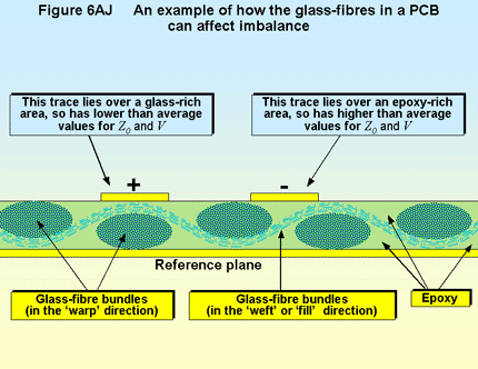
Also, a trace route that lies over a glass-rich area will have a slower V than the average for the PCB, whereas a route over a resin-rich area will have a higher V than the average. This will cause a skew between the two signals in the differential line that will tend to close their ‘eye pattern’ and increase emissions. The amount of skew can be as much as 5% of tp, the propagation time along the trace (sometimes called ‘flight time’ tflight) and can ruin attempts to minimise skew by trace length matching, especially important for EMC for differential pairs.
Of course, where the actual glass fibres will run in a PCB is unknown, and will vary between otherwise identical PCBs cut from the same FR4 panel and delivered in the same batch. Batch sampling using ‘test traces’ (see earlier) cannot deal with this problem. The usual way of overcoming this problem (without using non-woven dielectrics, see below) is to route all critical transmission lines – and all differential lines – at angles of between 30° and 60° to the warp or weft of the glass fibres in the PCB, so that the effect of the woven substrate cancels out sufficiently well [32].
Another technique is to make the spacing between traces whose propagation time is to be matched equal to the spacing between the glass bundles in the PCB material. Maybe someone will develop a non-woven glass-fibre PCB material that uses short lengths of glass randomly dispersed throughout the epoxy. [33] shows that PCBs based on glass fibre will have seriously difficulties with signals at 10Gb/s or more on traces longer than 600mm (e.g. in a backplane) even when using the above techniques. It is proposed that electronic deskewing should be used for higher data rates if woven glass-fibre is to be used for low-cost, but this would not help EMC.
Non-woven substrates are preferred, but such dielectrics are usually more costly than woven glass-fibre types. A way of obtaining the benefits of non-wovens whilst keeping costs low is discussed next.
5.2 Other types of PCB dielectrics
The death of FR4 and similar glass-fibre materials has long been predicted, but the alternative homogenous materials (such as pure polymers) are so much more costly that people keep on finding new ways of continuing to use them. Suppliers of homogenous dielectrics, often called microwave substrates, include WL Gore and Rogers Corporation.
One recent technique is to use one or two layers of a less lossy dielectric than FR4 (e.g. WL Gore’s “Speedboard C” prepreg in [35], GETEK in [11]) as a part of a stack-up that is predominantly FR4, as shown by Figure 6AK. This only adds a little extra cost compared with the traditional alternative of using all polymer layers, but not all PCB manufacturers may be able to successfully laminate different materials to create reliable PCBs. Accelerated life testing may be required to feel confident that such stack-ups will last the expected life of the product.

6 Matched-impedance connectors
Transmission line traces that must connect to a device, or exit one PCB to connect to another (or to a cable) must retain the same characteristic impedance if excessive reflections are to be prevented, and good SI and EMC achieved. The effects of a poor mismatch can be seen in the TDR plot of Figure 6E, where the initial connection between the cable and the PCB can be seen to have a very much lower impedance than the 50Ω trace being tested.
This mismatch does not matter to TDR measuring equipment, but in a real system it would cause significant SI problems for signals or noises with rise/fall times under 300ps (or sinewaves over 1GHz) and EMC problems with even slower (or lower frequency) signals or noises. [11] describes using Teradyne VHDL-HSD connectors in a backplane system using LVDS at up to 5Gb/s. It includes TDR simulations for 100ps rise/fall times and real measurements of eye patterns and impedances.
A great deal has been written about the design of matched-impedance PCB connectors (such as the type shown in Figure 6AD) and their development (for example [23]) but further discussion is outside the scope of this article.

As well as having the correct Z0s the connector pins used for differential signals should maintain the same path lengths for the + and – signals, which may mean buying connectors specifically designed for that purpose. Notice that differential transmission line connectors are all specified by Z0, but this is only their DM Z0 – their CM Z0 is not part of their specification, and is almost certain to differ from the CM Z0 of the differential traces on the PCB. This will create an impedance discontinuity for CM currents which could be bad for EMC and may even be bad for SI, especially if CM currents are high due to poor line balance.
This is a reason for at least making provision for filtering when differential traces must leave a PCB and pass through a connector and/or a cable – whether the connectors/cables are shielded types or not. Filtering transmission lines at off-board connectors was discussed earlier, and Figure 6AB gave an example of a layout for a filtered differential line and unshielded cable.
7 Shielded PCB transmission lines
7.1 ‘Channelised’ striplines
A stripline can be ‘channelised’ by running a ‘wall’ of via holes along both sides of the trace to create what is almost a shielded conductor inside a PCB, as shown in Figure 6AL. Sometimes designers route return traces either side of the signal trace on the same PCB layer to make a ‘shielded coplanar line’, otherwise described as a coplanar stripline. The via walls would follow the route of these coplanar traces, making it a channelised coplanar stripline.

This can be a very useful technique when crosstalk from a high-threat trace (such one carrying the output signal from an RF power amplifier to an antenna) into a nearby trace needs to be reduced. To be effective at reducing crosstalk, the via holes must be spaced no further apart than λ/10 at the highest frequency of concern (= 1/πtr where tr is the real risetime, not the data sheet specification) – and preferably a lot closer.
Channelised coplanar stripline techniques can also be used for differential lines, taking great care to maintain the line balance within the shielded coplanar channelised structure. As well as reducing crosstalk, such structures help prevent external influences (such as a mass of metal, PCB edge or a nearby gap in a plane) from affecting the characteristic impedance or unbalancing a differential line. The author doubts whether there are any equations for working out the Z0 of a channelised transmission line, or a coplanar channelised line, and because its structure is not the same from point-to-point along the length of the trace a 3D (rather than 2D) field solver would probably be required.
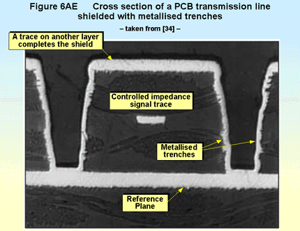
7.2 Creating fully shielded transmission lines inside a PCB
Some PCB manufacturers can now create linear trenches between layers in a PCB, plate them with copper and fill them back up with epoxy. As Figure 6AE shows, these can be used to create well-shielded transmission line traces inside a PCB that have much lower crosstalk and much better EMC than ordinary transmission lines [36].
[37] gives a formula for calculating the characteristic impedance of such PCB structures, but it suffers from the simplifying assumptions required to create any EMC formulae, so might not achieve good enough matching for modern high-speed PCB interconnections.
8 Miscellaneous related issues
8.1 Impedance matching, transforming and AC coupling
Networks of resistors can be used to connect a line with one Z0 to a line with a different Z0. These are usually called ‘matching pads’ and their design is described in the short article “Matching Pads” in [12]. Transformers can also be used to transform the Z0 of one transmission-line to match the Z0 of another, by varying the ratio of the windings between primary and secondary. These impedance transformers are sometimes called baluns because they can also be used to convert from single-ended to differential transmission, or vice-versa (balun = balanced-to-unbalanced transformer).
As mentioned earlier in the section on terminating a transmission line, accurate matching is necessary when connecting two lines with different values of Z0. Matching which gives an acceptable waveform for SI purposes might not be accurate enough for good EMC. The use of a magnetic close-field probe (see earlier) on a simple trial PCB will help prove how accurate the matching needs to be.
Transformers can be used to ‘float’ a differential signal so that it is not connected to any reference voltage in either the driver or receiver. This is used in long cable-based transmission lines (such as Ethernet) to ‘break the ground loop’ caused by differences in the ground potential between widely separated parts of an installation, so the signal is less corrupted by ‘ground noise’.
Galvanic isolation by transformers (floating) is also used to help prevent overvoltage damage and electric shock hazards due to the ‘ground lift’ caused by electrical faults and thunderstorms – but the transformers should be tested and approved to the appropriate ‘withstand’ voltage according to appropriate safety standards, such as EN 60950.
When using transformers in a signal path it is important that the average d.c. content of the signal is close to zero. Any d.c. content will magnetise the transformer’s core, and if the d.c. content is enough the magnetisation will be sufficient to distort the signal as it passes through the transformer. A similar problem arises when a series capacitor is used to a.c. couple signals or data. In this case, if the d.c. content is not zero the capacitor will charge up (or down) and it is possible that its voltage will exceed the common-mode range of the receiver and impair signal quality.
There are numerous protocols for encoding serial data so that its d.c. content averages to zero, refer to “When to use AC coupling” in [12].
8.2 A ‘safety margin’ is a good idea
Real rise/fall times of around 300ps are not unusual at the time of writing, and they are heading inexorably downwards as 90nm silicon processes are starting to appear in volume-produced devices, and as developments promise devices based on in 65nm and 45nm processes in just a few years. As Figure 6E above shows, the rise/fall times of such signals is small enough that a single via hole can create an impedance discontinuity that can cause reflections that distort waveshapes, close eye patterns, increase emissions and worsen immunity.
‘Die shrinks’ by IC manufacturers during a product’s production lifetime can reduce driver rise and fall times. So where a new design is initially acceptable but doesn’t have a large margin, poorer EMC and even increased unreliability could occur after a year or two’s production due to die-shrunk ICs being provided in place of the expected parts.
Die-shrunk ICs are supplied with exactly the same part number and packages as the original slower parts – only the batch numbers reveal their true nature – and only then to someone who knows at what batch the die shrink was implemented. Some IC suppliers have agreements with their customers to provide samples of die shrunk parts 6 months before they appear in normal shipments, so that any design modifications found to be needed can be done in time.
But 6 months is not a long time, and the author knows of one large manufacturer who used tens of millions of a particular microprocessor in a very wide range of products which each had production lifetime of over 4 years. A die shrink in that particular device resulted in all of their products having to be redesigned for EMC compliance, which took over two years to complete at a cost to the manufacturer of tens of millions of US Dollars.
So it is a good idea to try to find out what die shrinks are likely to occur in the IC’s being designed into a new product, over its likely production lifetime, then use the likely die-shrunk values for rise/fall time when designing the circuit and the transmission lines for its PCB.
It is better to use ICs whose drivers have a specified slew-rate – instead of the more usual ‘switch as fast as the silicon allows’ types. Die shrinks will have no effect on their rise/fall times – although the amplitude and frequencies of their core noises might be increased.
8.3 Filtering
Where the fastest rise/fall times or highest data rates or frequencies are not really required, it is usually possible to use low-pass filtering on the signals or noises – slowing down their transitions and/or reducing their highest frequencies. It might be practical to filter a driver output so much that transmission line techniques are not required at all, even for good EMC. This is a common technique for ‘static’ digital lines such as resets.
If matched transmission lines are required, the aim of filtering would be to make the rise/fall times of the signals or noises long enough to ‘smooth out’ the impedance discontinuities along a transmission line, making design much easier and improving SI and EMC (compare the impedance discontinuities seen by the 1ns and 150ps rise/falltime signals in Figure 6E). If rise/fall times can be limited to no less than 1ns (or maximum sinewave frequencies to 320MHz) much of the finer detail about designing transmission lines in this article can often be ignored.
Capacitors should not be used alone as filters for signal traces. Observing the voltage waveform on a trace with an oscilloscope it will be seen that adding capacitance at a device pin will slow down its rise/fall times and/or reduce its high frequency content. But what the ‘scope doesn’t show is that the added capacitor draws very high transient currents, increasing the magnetic field emissions from a PCB. These currents also increase the voltage noise between planes and so increase the emissions of electric fields from the plane edges. They also increase the levels of ground bounce and rail bounce noise that occur in the driver ICs.
So capacitors in filters should always be used with series resistances or ferrites to limit any increase in transient current. The values of the resistances or ferrites should be chosen taking the Z0 of the line into account.
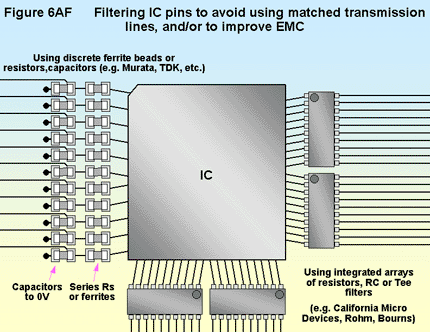
Some designers use filter capacitors with reflected wave switching – placing capacitors of between 4.7 and 22pF between the trace and the 0V plane immediately after the series resistors (on the load side) [39]. These capacitors can be left unpopulated, and if EMC problems arise various values can be experimented with to see which achieves good EMC without compromising SI by filtering too much.
8.4 CM chokes
Where the CM return path for a differential signal is not as good as it could be, CM chokes can be used to raise the CM impedance – reducing the CM currents, and so reducing the CM emissions. These chokes take up quite a lot of PCB space, and are not low-cost components, so they tend to be used where a differential line exits a PCB into an unshielded cable such as UTP, and so loses its reference plane (which is the current path for its CM noise).
CM chokes are also very important where coaxial connectors and cables are used for high-speed signals. Coaxial interconnections actually work in triaxial mode, with the wanted signal’s RF return currents flowing on the inside of the cable shield (due to skin effect) and the external RF noise currents flowing on the outside of the shield (also due to skin effect).
But all flexible coaxial cables suffer from leakage through the thickness of their shields which gets worse as frequency increases (some types more than others – expensive “superscreened” coaxial cables can be very good). It is generally found in practice that when using any types of flexible coaxial cables (other than superscreened) with data rates above 50Mb/s a CM choke is required to aid triaxial working and improve EMC. Part 1 of [1] and [2], especially its figure 11, show some relevant simplified schematics.
8.5 Replacing parallel busses with serial
Where the fastest edges or highest data rates or frequencies really are required for functionality, there is no choice but to deal head-on with all the imperfections in transmission lines and their terminations discussed in this article. Using classical line termination (see Figure 6J) helps a great deal, but if signal amplitude is not to be halved the driver circuit itself, inside the IC, must have pull-up and pull-down impedances that match the Z0 of the transmission line and output the full signal levels required by the load.
There are clever ‘microwave design’ tricks that can sometimes be used, such as adding a small stub to a trace to add inductance or capacitance (at a particular frequency) to compensate for an imperfection in the trace impedance, but these are limited in their scope and only work over narrow frequency bands.
The general way to deal with impedance discontinuities along a trace is to design them out. This is why the current trend is to replace multidrop parallel busses with point-to-point serial busses using low voltage differential signalling (LVDS) techniques, which use matched differential transmission lines. [9] shows that increasing the size of the antipads in the plane layers that the via hole passes through will reduce their capacitance so that they match the Z0 of the line better, but this is achieved at the expense of increased perforation of the 0V plane(s) – not a good thing for EMC. So when using signals with very fast edges or very high frequencies, for good SI and EMC we usually need to minimise the number of vias along a trace, ideally routing each such trace on a single PCB layer along its entire route.
If our differential lines are striplines routed completely on one layer, and their reference planes are unbroken for a large distance around the trace – then the only capacitive loading on the line will be from traces routed nearby on the same layer, and from nearby metal features that penetrate through the PCB, such as via holes and fixing screws. A number of other issues can still arise, such as the characteristic impedances and stub filtering effects of the via holes at the ends of the line, and the effects of routing variations and the warp and weft of the glass fibres, resin rich areas, etc.
Careful design of the layout and stack-up, and the use of computer-aided design tools, can reduce the significance of all these details and achieve serial data interconnections that will run at very high data rates with good EMC.
8.6 The lossiness of FR4 and copper
Copper traces laminated into FR4 PCBs have an increased surface roughness due to the woven glass fibres in the FR4 substrates. FR4 itself is a lossy dielectric, with approximately 10 times the ‘loss tangent’ of other PCB materials such as the microwave substrates made by Rogers Corporation (and others) and ‘pure polymer’ materials such as those used in microvia/HDI PCBs (see Part 7 of this series). For signals that are around 1GHz, these losses are generally only a problem for traces that are over 300mm long. Eric Bogatin of Gigatest Labs has a number of articles and presentations available on this topic [38], also see “Characteristic impedance of lossy line” in [12].
Pre-emphasis is often used to compensate for the low-pass filtering effects of FR4 at gigabit data rates. Pre-emphasis boosts the drive levels in such a way as to compensate for the filtering effects of extended PCB traces. For example, with pre-emphasis, serial busses such as Xilinx’s Rocket I/O claims to reliably support speeds of 3.125 Gb/s over transmission lines of at least 500mm in FR4.
At first sight, pre-emphasis appears to be solely an SI issue, not an EMC one, but pre-emphasis means boosting the amplitudes of at least the 3rd and 5th harmonics of a signal, which could lead to increased emissions at those frequencies.
8.7 Problems with coated microstrip
Figures 6A and 6Z show some examples of coated microstrips used for single-ended or differential transmission lines. The usual coatings are solder resists (solder masks) and component legends (sometimes called the ‘silk screen’ layer), although some PCBs are conformally coated to protect from moisture, and/or encapsulated to protect from shock and vibration.
But the dielectric constants and loss factors of many such coatings are not very well characterised at high frequencies, and the thickness of coating applied is often not very well controlled [31]. In addition, most PCB specifiers only specify the solder mask by its solder-resisting qualities, leaving the PCB manufacturer free to substitute various alternatives. This can obviously cause variations in transmission line matching between different PCBs, and possibly over the width or length of a single PCB.
One way of dealing with this problem, suggested by [31], is to ensure there are no coatings or printed legends over any microstrip lines. Another way is to include a number of test coupons (see above and [15]) at widely-spaced locations on the PCBs and test them against specific performance targets at Goods Receiving before accepting each batch. Actually specifying the solder mask and legend materials by their manufacturers’ part numbers should also help maintain quality.
8.8 The effects of bond-wires and leads
In the past, it has been normal to treat the pin of a driver or receiver as the end of a transmission line. But as rise/falltimes reduce the lengths of the leads (pins) and bond wires associated with a device are becoming more significant.
With very fast risetimes, and/or devices that use very large packages (with long lengths of leads or bond wires), it is possible for a signal waveform to be measured as perfect at it’s pin’s solder joint to a PCB, but the actual waveform applied to the silicon is degraded. Conversely, the waveform at a pin can appear degraded whilst the waveform applied to the silicon is good (see “What’s that Plateau?” in [12] for an example). When a device is attached to a stub, the length of its lead and bond wire can make the true length of the stub much greater than it appears from the PCB layout – so that it may no longer be able to be treated as a simple capacitive point load.
9 Simulators and solvers help design matched transmission lines
Part 1 of this series shows that where it is very important for commercial success to get to market quickly with low-cost-of-manufacture products – the EMC of the PCBs needs to be good and ‘correct-by-design’. It is also important to realise, as Eric Bogatin often points out in his articles and presentations on SI [38], that any equations and formulae that can reasonably be written down and worked out with a calculator are only useful for first-order approximations, initial order-of-magnitude design estimates, and ‘sanity checking’ the results from computer-aided design tools.
This article shows that designing and matching transmission lines with the accuracy required for good SI when using modern digital ICs and high data rates, and for good EMC, requires attention to a great deal of detail. People aren’t good at handling such detail – but computers are. Without appropriate computer aids (and measurement technologies such as TDR, see above) it is normal for at least two PCB iterations (re-spins) to be required to achieve the desired EMC performance at low cost, but the time this takes is becoming an increasing problem for commercial success. Many designers wind up sticking extra shielding and filtering onto their products in a panicky attempt to hit their new product’s market window – regardless of the cost.
It is probably impossible to design (for example) a PCB that uses 2.5GHz serial interconnections and get its SI and EMC right enough first time, without intelligent use of computer-aided design tools, including at least a 2D field solver (maybe a 3D one). But such computer aided design tools are now available, and getting much more useful every year. Now we can solve all (or most) of our detailed design issues in the virtual world before laying out and making the first PCB.
Computer-based simulators for calculations of PCB transmission line impedance have been available for many years, but user-friendly simulators that run on standard PCs, deal with the detail we require, and give reliable answers are now becoming available. A number of companies offer such products, but the ones that seem to be mentioned most in papers presented at EMC conferences are from Polar Instruments [23], Hyperlynx (e.g. available from Mentor Graphics) and Ansoft (Google easily finds their websites).
A new product called EMI Stream works at the component placement design stage (pre-routing), and claims to help find optimal placement locations and optimal routing for good EMC. It also claims to help suppress resonances between power and 0V [40].
Ideally, we would want to be able to extract accurate trace parameters from a simulation of a PCB layout that addresses all of the detailed issues discussed above; use those parameters in a circuit simulations, and iterate between the PCB layout and the circuit simulator until SI requirements are satisfied (as discussed in Part 1 of this series [6]). Then we would want to simulate the EMC characteristics of the whole PCB in its final assembly and predict what its emissions and immunity were going to be when measured with an antenna at 10m.
Unfortunately, not all of the tools required to do all this exist – or if they exist they don’t yet permit a fully ‘joined-up’ virtual design process. An example of good practice and use of computer tools that were current in 2001 is given in [11]. However, computer-aided design tools that exist at the time of writing do permit complete virtual design of SI. Since high-frequency SI and EMC are essentially the same issues [7], we can use SI design tools with tougher SI requirements than are needed for functionality to improve a PCB’s EMC characteristics.
At the time of writing, it is strongly recommended that – if the time it takes a signal’s edge to travel along the full length of the trace (the trace propagation time, tp, see above) is longer than 1/6th of the signal’s rise/fall time (whichever is the shorter) – the entire signal path should be simulated. Simulation can use the transmission line facilities in IBIS or SPICE-based circuit simulators, or other types of simulator, to see whether a transmission line is needed for SI.
All clock and data strobe paths should always be simulated. They will almost certainly need to use a matched transmission line for good EMC, helping to reduce the need for expensive shielding and filtering.
Intel application notes recommend using a loss factor of 1.0Ω thou2/inch for copper in FR4. This is higher than the published figure of 0.662Ω thou2/inch for annealed copper, due to the additional surface roughness caused by pressure lamination and FR4’s woven glass-fibre substrate. If using non-woven substrates the standard published figure should be used instead.
10 EMC-competent QA, change control, cost-reduction
See section 8 of Part 3 of this series [19] for a discussion of this important issue.
11 Compromises
It is easy to write an article like this and simply list all of the relevant good EMC design techniques – but in real-life there are a great many design compromises to be made, and this is where the circuit and PCB designers really earn their keep.
Designers are often put under cost or time pressure by managers who don’t understand the technical trade-offs, and so don’t understand that their actions could have the opposite effect to that which they intend and actually increase project costs and delays, as well as maybe increasing manufacturing and warranty costs. For more on this topic, please refer to part 1 of this series [6], plus the final section of part 2 [8].
12 References
[1] “Design Techniques for EMC” (in six parts), Keith Armstrong, UK EMC Journal, Jan – Dec 1999
[2] “Design Techniques for EMC” (in six parts), Keith Armstrong, http://www.compliance-club.com/keith_armstrong.asp
[3] “PCB Design Techniques for Lowest-Cost EMC Compliance: Part 1”, M K A