Design Techniques for EMC Part 4 - Shielding (part 2)
This is the fourth in a series of six articles on basic good-practice electromagnetic compatibility (EMC) techniques in electronic design, to be published during 2006-7. It is intended for designers of electronic modules, products and equipment, but to avoid having to write modules/products/equipment throughout - everything that is sold as the result of a design process will be called a ’product’ here.
This series is an update of the series first published in the UK EMC Journal in 1999 [1], and includes basic good EMC practices relevant for electronic, printed-circuit-board (PCB) and mechanical designers in all applications areas (household, commercial, entertainment, industrial, medical and healthcare, automotive, railway, marine, aerospace, military, etc.). Safety risks caused by electromagnetic interference (EMI) are not covered here; see [2] for more on this issue.
These articles deal with the practical issues of what EMC techniques should generally be used and how they should generally be applied. Why they are needed or why they work is not covered (or, at least, not covered in any theoretical depth) - but they are well understood academically and well proven over decades of practice. A good understanding of the basics of EMC is a great benefit in helping to prevent under- or over-engineering, but goes beyond the scope of these articles.
The techniques covered in these six articles will be:
- Circuit design (digital, analogue, switch-mode, communications), and choosing components
- Cables and connectors
- Filtering and suppressing transients
- Shielding (screening)
- PCB layout (including transmission lines)
- ESD, surge, electromechanical devices, power factor correction, voltage fluctuations, supply dips and dropouts
Many textbooks and articles have been written about all of the above topics, so this magazine article format can do no more than introduce the various issues and point to the most important of the basic good-practice EMC design techniques. References are provided for further study and more in-depth EMC design techniques.
Table of contents for this article
4. Part 4 - Shielding (screening)
Published in previous issue 69 March 2007
4.1 Introduction
4.2 Shielding with metal plates
4.3 Volumetric shielding of products
4.3.1 Nested shielding and cost-of-manufacture
4.3.2 General concepts in volumetric shielding
4.3.3 Skin effect and absorption
4.3.4 Very low frequency shielding
4.3.5 SE is compromised by leakage from apertures
4.3.6 The resonant/antenna behaviour of a single aperture in the far field
4.3.7 Multiple apertures in the far field
4.3.8 Cavity resonances and aperture leakage
4.3.9 Near-field leakages through apertures
4.3.10 Designing to reduce aperture leakages
4.3.11 Waveguide-below-cutoff techniques
In this issue
4.3.12 Shielding of displays (and the like)
4.3.13 Shielding membrane switch panels
4.3.14 Shielding ventilation apertures
4.3.15 Shielding rotating metal shafts that penetrate an enclosure
4.3.16 Combining heatsinking with enclosure shielding
4.3.17 Preventing shield degradation from conductor penetrations
4.4 Shielding at PCB level
4.4.1 Reasons for shielding at PCB level
4.4.2 Overview of techniques for PCB level shielding
4.4.3 Types of PCB shielding-can
4.4.4 Methods for bonding shielding-cans to PCB planes
4.4.5 Suitable materials for PCB shielding-cans
4.4.6 Apertures in PCB shielding-cans
4.4.7 Waveguide-below-cutoff methods in PCB-level shielding
4.4.8 Cavity resonances in PCB shielding-cans
4.4.9 Shielded cables and traces entering/exiting PCB shielding-cans
4.4.10 Combining filtering with shielding at PCB level
4.4.11 Combing heatsinking with shielding at PCB level
4.5 Estimating shielding effectiveness with PC-based simulators
In the next issue
4.6 EMC gaskets
4.6.1 Volume-conductive elastomers
4.6.2 Conductively coated or wrapped elastomers, see Figure 4BH
4.6.3 Metal (wire) meshes, see Figure 4BJ
4.6.4 Spring fingers (’finger stock’), see Figure 4BK
4.6.5 Some other types of gaskets 4.6.6 Mechanical design techniques for gaskets 4.6.7 Gasket clamping
4.7 Materials useful for shielding
4.7.1 Metals and their surface finishes
4.7.2 The problems of polymer passivation
4.7.3 Metallised papers and fabrics
4.7.4 Paints and lacquers
4.7.5 Painted or plated plastics
4.7.6 Shielding with volume-conductive plastics
4.7.7 Alternatives to shielding plastic enclosures
4.7.8 Environmental considerations
4.7.9 Preventing corrosion
4.8 References
4.9 Acknowledgements
4. Part 4 - Shielding (screening)
4.3.12 Shielding of displays (and the like)
Displays require apertures in enclosures, compromising shielding (see 4.3.5 in the first half of this article [20]). Individual holes for a few tiny indicator lamps or LEDs may not degrade SE too much for some types of commercial or industrial equipment, but for improved SE they can be...
- fitted with tiny metal-film or mesh shielded windows (see below)
- located behind a clear area in a shielded membrane panel (see 4.3.13)
- located at the far end of a metal tube that is swaged or otherwise 360ø metal-to-metal bonded to the conductive surface of the enclosure to make a waveguide-below-cutoff (see 4.3.11 in [20]), as shown in Figure 4AE

Figure 4AE Waveguide-below-cutoff techniques for indicators using LEDs or small lamps
The technique shown in Figure 4AE adds to the cost of the shielded enclosure, but allows low-cost surface-mounted LEDs to be used and does not require very close alignment of a leaded LED with a hole in a metal panel, so reduces assembly time and rework.
Pointing an infra-red or optical transmitter through a waveguide-below-cutoff as shown in Figure 4AE is a wonderful method of communicating data, up to Gb/s rates if using a laser. Microwave transmitters that operate above the waveguide’s cut-off frequency can also communicate through a shield in this way without degrading the SE.
Mounting a display outside a shielded enclosure avoids the aperture, but of course the display is no longer benefiting from the enclosure shielding, and to preserve the shielding of the enclosure the display’s data and power cables must be filtered at the point where they exit the shielding enclosure (see 4.3.17 and 4.3.18).
Where an aperture large enough to compromise SE is necessary, the ’dirty box’ method shown in Figure 4V of [20] can be used. The dirty box is effectively an extension of the shielding surface of the clean box. EM fields from the external EM environment are present inside the dirty box, so it does not provide shielding for any displays located inside it.
The dirty box must make a good RF bonds along all its contact areas with the inside of the clean box, to prevent the creation of apertures that could ruin the SE of the clean box. Frequent fixings around its periphery are necessary, with gaskets too if high SE values are to be achieved or frequencies of more than about 300MHz are to be shielded. Appropriate design guidance was provided in 4.3.5 - 4.3.11 of [20].
Of course, the display mounted in the dirty box is not protected by any shielding, so it must have low enough emissions and high enough immunity in its own right. The cables from the dirty box to the clean box compromise the SE of the enclosure, so a filter is usually required at the point where the cable enters the dirty box. Because the cable lengths in the dirty box are quite short they usually only create emissions or immunity problems at higher frequencies, so the filtering required can often be just an RF-suppressing ferrite cylinder fitted very close to the point of penetration of the dirty box, but a feedthrough filter fitted to the dirty box itself may be needed (see 4.3.17 and 4.3.18) to provide higher attenuation.
Where a display must be fitted inside a shielded enclosure, shielded windows are usually needed to prevent its visual aperture from degrading SE by too much. Some high-grade CRTs can provide a good shield when the metal frame around the front of their tube is electrically bonded to the front panel all around the aperture. Active matrix LCDs upgrades to products which had used high-grade CRTs have been known to be the cause of more emissions than the CRTs, and some have needed additional shielded windows where the CRTs had not.
A variety of shielded windows are available, based on two main technologies:
- Thin metal films, usually indium-tin-oxide (ITO), coated onto clear plastic sheets. At film thicknesses of 8μm and above, optical degradation starts to become unacceptable; and for battery-powered products the increased backlight power may prove too onerous. As Figure 4G of [20] shows, the thickness of these films may be insufficient to provide good SEs below 100MHz.
- Embedded metal meshes, usually a fine mesh of blackened copper wires. For the same optical degradation as a metal film these provide much higher SEs, but they can suffer from Moir‚ fringing with the display pixels if the mesh elements are not sized correctly. It can also help if the mesh is diagonally oriented with respect to the rows of pixels or dots in the display.
Figure 4AF shows an example of the visual obscuration created by two kinds of metal mesh window, and Figure 4AG shows some examples of the SE provided by metal film and metal mesh windows.
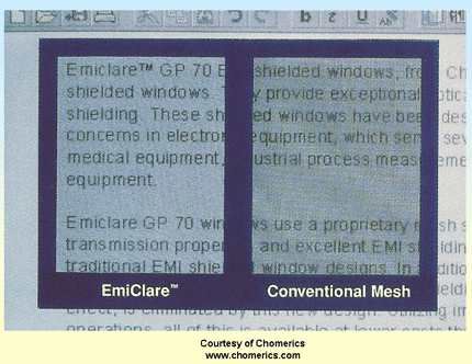
Figure 4AF Two examples of metal mesh shielded window materials
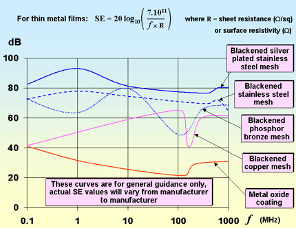
Figure 4AG Some examples of SEs provided by metal film and mesh shielded window materials
A vital issue for screened windows is that their conducting material must be RF-bonded directly to the enclosure shield’s conductive surface around all the edges of the display aperture (known as 360ø bonding), so conductive gaskets are generally required. This is so that the surface currents on the inside and outside of the shielded enclosure (see Figure 4F, [20]) flow relatively unimpeded across the display shield.
Film-coated plastic sheet used as a shielded window may need to be mounted in a metal frame that provides sufficient stiffness for compressing a conductive gasket (see 4.6) between its conductive surface and the conductive surface of the shielded enclosure, all around their perimeter. Where an LCD display is used, its own frame is often stiff enough. Windows with embedded films or meshes are thicker, and if thick enough might be stiff enough not to need any additional stiffening.
Figure 4AH shows an assembly method that uses conductive sealants or conductive adhesives to avoid the need for mechanical fixings. The sealant or adhesive does not need to be compressed, making mechanical design much simpler. The use of UV-curable sealant or adhesive can reduce assembly times and the result for both shielding and environmental sealing can be better mechanical fixing methods, at lower cost. Conductive double-sided adhesive tape could be used instead, which has the advantage of not requiring a cure time, although unless it is die-cut (with no joints) its environmental protection will not be as good. 
Figure 4AH Example of RF-bonding a shielded window
Figure 4AJ shows an example of a mesh-shielded display window with an embedded mesh (such as the one sketched in Figure 4AG) just after assembly, before the excess mesh has been trimmed off. The step around the side where the metal mesh is exposed is visible.
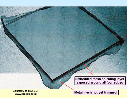
Figure 4AJ Example of a mesh-shielded window, before assembly
Metal films and meshes must be very thin if they are to be seen through at all, and this limits the amount of absorption loss they can provide (see 4.3.3 in [20]). Honeycomb metal display shielded windows, similar to the ventilation panels shown in Figure 4Z, are also available for the very highest performance. These are large numbers of waveguides-below-cutoff stacked side by side (see 4.3.11 in [20]), and are mostly used in security or military applications where their extremely narrow viewing angle means that the operator’s head prevents anyone else from sneaking a look at their displays.
’Nanoscale’ assembly techniques are being developed that use multiple very thin conductive films separated by very thin dielectric layers. The spacing between the layers is chosen so that a desired range of optical wavelengths passes through without significant attenuation, whereas other frequencies of radiation (such as RF) experience strong attenuation. The layer spacings can be set to pass the visible spectrum (e.g. for displays, illumination, etc.) or certain ranges of infra-red or ultra-violet wavelengths appropriate for optical data communications or certain kinds of measuring instruments.
4.3.13 Shielding membrane switch panels
Membrane panels are laminated plastic constructions with embedded pushbuttons, clear areas for LEDs and displays to be seen through, etc. They often cause problems for enclosure SE, because of the apertures cut out for them in the enclosure. They usually have an aluminium backplate, with a fixing point (mounting) at each corner. Even when the fixings make a good RF bond (which they often do not) they create four long apertures around its edges of the membrane panel.
The solutions are similar to those already described for displays in 4.3.12:
- Mount entirely outside the enclosure and filter the cable from the panel at the point where it enters the enclosure, with at least an RF-suppressing ferrite cylinder (but feedthrough filters may be required)
- Use the dirty box technique (see Figure 4V in [20])
- Fit a shielded window layer (metal film or mesh) in the panel and RF-bond it to the conductive surface of the metal enclosure all around the edges of the aperture. In this scheme the membrane panel becomes the shielded window for any displays.
4.3.14 Shielding ventilation apertures
Methods of shielding ventilation apertures are similar to those used for mesh-shielded windows, except that the mesh size can be much larger to present less impedance to the airflow. Expanded or perforated metal is often used, and because they are thin their SE is mostly given by reflection rather than by absorption, so they are good for screening low frequency E fields but poor for low frequency H fields. Shielding of plane (far field) waves is generally acceptable for most purposes providing the aperture dimensions are less than one-hundredth of the wavelength at the highest frequency of concern (see Figures 4J and 4M of [20]).
Round, square or hexagonal holes/mesh shapes are much better than rectangular or slot apertures with the same area. The perpendicular elements of a mesh must make reliable electrical contact at all crossing points (e.g. by welding). High levels of SE may need much smaller apertures, or a different technique such as the ’wire wool’ sandwich shown in Figure 4AK.
Waveguide-below-cutoff techniques (see 4.3.11 in [20]) are often used for shielding ventilation apertures, see Figure 4Y, Figure 4Z and Figure 4AA all of [20], and Figure 4AK. Many honeycomb metals have cells that are glued together, in which case their SE can be improved if the honeycomb and its frame is plated with metal after assembly.
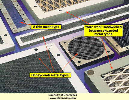
Figure 4AK Some types of ventilation shields
Like shielding windows, all vent shields must make electrical contact around their periphery to the aperture in their shielded enclosures. For low values of SE or low frequencies, a metal fixing every 100mm may be adequate, but for high values of SE or frequencies of 1GHz or more conductive gaskets will probably be needed, clamped between the vent and the enclosure shield.
At least one manufacturer of highly shielded 19" rack cabinets uses a waveguide-below-cutoff technique for its top and bottom ventilation apertures, similar to Figure 4AC of [20] but with metal spacers instead of spring fingers to give a gap about 10mm tall for good airflow.
Ventilation shielding is complicated by the need to clean the shield of the dirt deposited on it from the air that passes through. Adding removable air filters can allow the ventilation shielding to be fixed permanently fixed in place.
4.3.15 Shielding rotating metal shafts that penetrate an enclosure
Rotating metal shafts can enter/exit shielded enclosures for power transmission, or for control (e.g. potentiometer shafts). These are conductors and therefore can be just as bad for SE as a cable which is neither filtered nor shielded (see 4.3.17 and 4.3.18), so may need to be fitted with conductive gaskets.
Special types of gaskets are required to avoid friction and wear when shafts rotate, whilst still maintaining good electrical contact. Conductive grease can be used, usually filled with silver or carbon particles. Metal bearings do not make electrical contact between a shaft and its frame, because they always ride on a film of grease, so they will probably require conductive grease.
A better method is to use plastic shafts. Where low values of SE are required below 1GHz their apertures might be small enough to be acceptable, but for high SE and/or >1GHz the shaft should pass through a waveguide-below-cutoff (see in 4.3.11 in [20] and Figure 4AE), remembering that the plastic shaft will reduce the waveguide’s cutoff frequency.
Similar methods can be used for other metal or non-conductive items that must penetrate a shielded enclosure and be free to move physically.
4.3.16 Combining heatsinking with enclosure shielding
Figure 4AL shows one way in which shielding and heatsinking can be combined, in this case for power devices. The devices use the rear wall of the shielded enclosure as their heatsink, and a finned heatsink could be attached to the outer surface of the wall (with a suitable thermal grease to aid conduction from the wall).
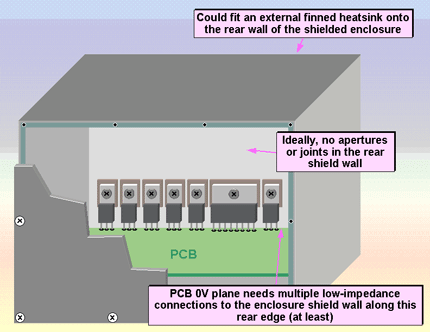
Figure 4AL An example of combining shielding and heatsinking
The stray capacitances from the devices inject high levels of RF currents into the shield wall, which for good EMC (and reduced internal crosstalk) must be returned to the circuits on the PCB with the smallest loop area. This is achieved by RF-bonding the PCB’s 0V plane to the rear wall, using (for example) a number of spring fingers soldered along the rear edge of the PCB. Another method is to extend the 0V plane into an edge-plated strip along the rear edge of the PCB, and pressing that edge against a strip of conductive gasket on the rear wall when the PCB is assembled in the enclosure.
Where the 0V plane is not the optimum path for the returning currents, RF-bond the correct PCB conductor to the rear wall in a similar manner, via a number of series capacitors spread along the edge. Where safety is an issue - the values, ratings and safety approvals of the capacitors will be important.
4.3.17 Preventing shield degradation from conductor penetrations
It was mentioned in 4.3.2 of [20] that the SEs of all real shields are compromised by apertures (seams, gaps, joints, displays, etc.) and cable penetrations. Section 4.3.5 and subsequent text in [20] covered the design techniques for apertures, and this section is concerned with design techniques for conductor penetrations. Figure 4AM shows the general philosophy - all conductors that penetrate a shielded enclosure must be RF-bonded to the shield wall at their point of penetration using one of the following methods...
- RF-bonded directly (i.e. metal-to-metal) to the shield wall at the point of penetration (for the earth/ground connection and other conductors that can be earthed/grounded)
- Filtered, with the metal body of the filter RF-bonded (metal-to-metal at multiple points, or 360ø using a gasket) to the shield wall at the point of penetration (for unshielded signal, data, control or power conductors). Feedthrough or through-bulkhead filters are necessary where high attenuation is required above 100MHz.
- Shielded, with the cable shield 360ø bonded metal-to-metal to the shield wall at point of penetration (for any signal, data, control or power conductors)
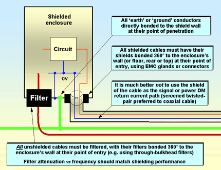
Figure 4AM Bonding, filtering or shielding all conductors that enter/exit a shielded enclosure
Section 4.3.15 discusses techniques appropriate for conductors (such as rotary shafts) that penetrate shields, but are not wires or cables carrying signals, data, control or power.
Details of the correct design techniques for filters that penetrate shield walls are covered in 3.3 of [3]. Details of the correct design techniques for shielded cables that penetrate shield walls are covered in 2.6.5 to 2.6.7 of [4]. Notice that it is best to use the cable shield only for the control of interference - not for carrying signal or power return currents, so coaxial cables are not recommended for EMC (see 2.6.2 and 2.6.3 of [4]).
It is very important indeed to make sure that no conductors of any type enter a shielded enclosure without being treated by one of the methods above. It doesn’t matter what the purpose of the conductor is. It is also very important to realise that at RF, and especially above 100MHz, even a very short piece of wire has too much impedance to be used as an RF bond. In the above bulleted list, where it says ’metal-to-metal’ - that is exactly what is required. No pigtails or connections via connector pins are acceptable.
In multiconductor cables with an overall shield it is common to find some or all of the internal conductors fitted with their own shields. These internal shields are mainly to reduce crosstalk between the internal conductors, so if they have their shields pigtailed or passed through connector pins it is not usually an important issue for EMC - as long as the overall cable shield is of sufficient shielding quality and terminated 360ø at the point of penetration of the shield.
I have often been asked to solve emissions/immunity problems where people had spent a lot of money on a shielded enclosure, and had done an excellent job of bonding, filtering or shield-bonding most of the cables that entered or exited the enclosure, but they hadn’t bothered to do anything with the mouse or keyboard cables, because they weren’t carrying high-speed signals - but of course this was the cause of their problems.
What matters is the CM noise, not the DM signals, and any conductor will behave like an ’accidental antenna’ for CM noise (see 2.2. of [4]), picking it up by conducted and/or radiated means on one side of the shielding barrier, and coupling it to the other side, compromising the shielding.
Field solvers discover this sort of problem very quickly. Figure 4AN shows a simulation of a floating wire that penetrates through a small ventilation hole in a shielded enclosure, and shows how it behaves like an antenna, coupling radiated fields from one side of the metal barrier to the other.

Figure 4AN Field solver simulation of a thin wire penetrating a shielded enclosure
4.4 Shielding at PCB level
Returning to the earlier theme of applying shielding at as low a level of assembly as possible to save costs (see 4.3.1 in [20]), this section discusses shielding at the level of the PCB, and is adapted from [21].
Shielding at enclosure level is unable to deal (on its own) with the increasing problems of interference between devices within products, due to continuing shrinking of the silicon feature sizes in integrated circuits (ICs) and the increasing packing density of modern surface-mounted printed circuit board (PCB) assemblies. The increasing use of embedded wireless communications, with its ’noisy’ transmitters and ’sensitive’ receivers exacerbates this problem.
As radio communications move into the microwave bands, and as ICs emit ever-higher levels at ever-higher frequencies, emissions regulations will soon be setting limits up to 2.7GHz (in Europe). But enclosure shielding is unsuitable for achieving significant levels of attenuation at such frequencies, without using costly, heavy and unattractive military design techniques.
PCB-level shielding is capable of dealing with problems of internal interference and regulatory emissions control at low-cost, providing a few basic design rules are followed. There are many interesting developments in PCB-level shielding technology, providing improved shielding performance with low-cost materials and ease of assembly.
Upcoming environmental legislation in Europe adds an extra dimension, with the need to employ shielding techniques that have low environmental and recycling costs.
4.4.1 Reasons for shielding at PCB level
There are many good reasons for using shielding techniques at PCB level. The most obvious one is that shielding always adds cost and weight but these disadvantages are minimised by shielding at the lowest level of assembly - the PCB.
The continued miniaturisation of surface-mounted devices (SMDs) and the increasing density of PCBs, are making it more necessary to shield different areas of a product from each other, to achieve the desired levels of functional performance in the product.
The continued shrinking of the silicon features in ICs is making them more susceptible to signal degradation. PCB-level shielding is a low-cost way to enable modern ICs to operate reliably in the noisy environment inside a typical modern electronic product.
When integrating wireless (radio) communications with a product, the close proximity of very ’noisy’ transmitting antennae tends to cause interference with sensitive circuits elsewhere in the product (analogue and digital devices can both be susceptible). The close proximity of very sensitive receiving antennae to ’noisy’ circuits such as switch-mode converters and digital processing can reduce the range over which the wireless communication will work. PCB-level shielding is a valuable technique for wireless communications.
Many modern portable computing devices are equipped with a variety of wireless data communications (such as Bluetooth, IEEE 802.11) but have no visible antennas because they are mounted inside the product’s enclosure. The enclosure clearly cannot be shielded, and so PCB shielding techniques must be used instead.
Regulatory issues are also significant. As ICs’ silicon feature sizes decrease, digital and switch-mode power devices switch faster. Digital processing speeds are also continually increasing. The result is that modern electronic products are increasingly emitting significant levels at frequencies exceeding 1GHz. But the spectrum above 1GHz is increasingly being employed for personal communications, so regulatory emissions standards are moving to protect the radio spectrum up to 2.7GHz (in Europe), and beyond.
Modern product enclosures are perforated with increasingly large visual displays, connectors for numerous kinds of cables, slots for a wide variety of removable storage media, apertures for ventilation, and must be constructed with a number of joints for ease of assembly. At higher frequencies, constructional issues that were once negligible can seriously compromise shielding effectiveness (SE). PCB-level shielding-can be used to reduce the SE requirements for the overall enclosure, possibly even completely removing the need for enclosure-level shielding.
4.4.2 Overview of techniques for PCB level shielding
Figure 4AP provides an overview of the issues associated with PCB shielding. A five-sided conductive ’shielding-can’ is placed over an area of circuit on a PCB, and electrically bonded by via holes in the PCB at multiple points around its perimeter to a plane layer inside the PCB (or on its bottom layer). The result is a six-sided conductive enclosure, part of which is embedded in the PCB itself. Figure 4AQ sketches a cross-section of a similar PCB structure.
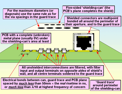
Figure 4AP Overview of PCB shielding and filtering

Figure 4AQ Cross-section of a PCB fitted with a shielding-can
The plane layer used is usually at 0V potential, but could be at any potential. Traces that enter or leave the shielding-can must be either shielded or filtered (Figure 4AP only shows filtered traces). If the plane is on an inner layer of the PCB, the traces and devices on the other side from the shielding-can are not shielded. If a circuit to be shielded has devices fitted on both the top and bottom of a PCB, both sides can be fitted with shielding-cans (and PCB plane layer may not always be required). But double-sided shielding-cans are more awkward for automated assembly.
Where the devices on the top and bottom of a PCB are associated with different circuits, they can be isolated from each other (to some degree) by using an internal PCB plane layer. It is also possible to fit shielding-cans over both of these circuit areas, each one using the same plane layer as its sixth side.
For more details on the PCB design techniques associated with shielding-cans, see 3.3 of [3], and Chapter 2.2 of [22].
Unfortunately, when using through-hole-plate (THP) PCB construction, the plated-through holes associated with the circuits on one side of the plane layer will protrude into the shielded volume on the other side of the plane layer, where they will ’crosstalk’ into its circuits. Also, the perforations in the common plane layer due to the clearance holes around the through-holes will reduce the SE between the top and bottom shielded volumes.
Microvia (HDI) PCB technology (see Chapter 7 of [22]) allows the achievement of much better isolation between two shielded volumes on opposite sides of a PCB, because it uses ’blind’ and ’buried’ plated holes that do not pass completely through the PCB. The use of microvia PCB construction (also known as high density interconnect [23], or sequential build-up) makes it possible for plane layers not to be perforated at all. Figure 4AR sketches the general principle, which should be compared with Figure 4AQ.
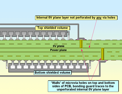
Figure 4AR Example of double-sided shielding using microvia (HDI) PCB technology
PCBs constructed using microvia technology can achieve very high levels of isolation between circuits assembled on opposite sides of a PCB with an unbroken internal plane layer between them.
4.4.3 Types of PCB shielding-can
Traditionally, PCB shielding-cans have been made of sheet metal, such as tin-plated steel, brass or beryllium copper. They had multiple pins around their perimeter for soldering into plated through-holes, and they usually had clip-on lids so that the devices inside could be accessed. The clip-on lids used multiple spring fingers around their perimeters to help minimise the resulting ’leaky’ shield gaps. They were also available with internal dividers that could shield two or more areas of circuitry from each other. Figure 4AQ shows some examples of PCB shielding-cans.
Surface-mounted metal shielding-cans have become readily available in recent years, and cans of up to 50mm square are successfully assembled automatically at the same time as other SMD parts. A number of alternative designs are now available (or are being developed) to reduce weight and cost. Also, shielding-cans with reduced ’environmental impact’ are becoming available.
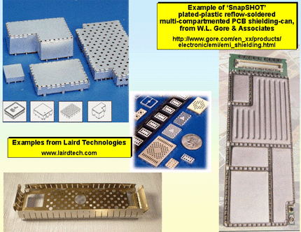
Figure 4AS Some examples of PCB-mounted shielding-cans
Metal shielding-cans without removable lids cost and weigh less, and have better SE because they have fewer apertures. Laird Technologies has a design that allows the top of the shielding-can to be removed with a ’key’, just like opening a traditional oblong tin of sardines. To repair the shielding-can, a new metal lid with conductive adhesive is pressed onto its body.
A variation on the shielding-can made from sheet metal is the die-cast metal ’maze’ base that is soldered or press-fitted to the PCB and has metal spikes along its top edge. A flat metal lid with holes at appropriate places is pressed onto the base. An example of a PCB using this technique is shown in Figure 4AT.
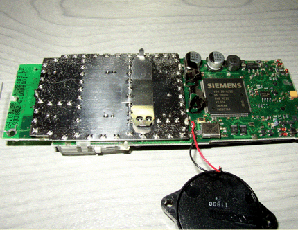
Figure 4AT Example of a DECT phone with a circuit area shielded by a die-cast ’maze’ with a pressed-on sheet metal lid
Plastic moulding techniques have recently become a vigorous area for research and development. Formed plastic shielding-cans have for years been painted with conductive adhesive, or had metal layers applied by vacuum deposition (such as sputtering) or electro-plating. But the tooling costs for the automated conductive coating of such parts can be high, or they can require costly manual processing.
One alternative is to print a flat sheet of plastic with a mesh or solid layer of conductive ink, usually silver [24], [25], or to plate it with metal [26], [27]. The conductively coated sheet is then cut and thermo-formed into the desired shape. The difficulty is in designing the ink or metal film so that it can stretch enough to make a wide range of PCB-level shielding shapes without cracking, since this creates apertures and reduces the SE.
Conductively coated plastic parts can be used just as they are, if stiff enough, but some types will need mechanical assistance, such as being clipped into a plastic or metal support (often created by the internal shaping of the product’s enclosure). An alternative is to use the thermo-forms made from the conductively coated plastic sheets as ’preforms’ for a plastic moulding process. This is sometimes called ’in-mould shielding’, with the shielding preform being moulded into the finished component, thereby avoiding the need for manual assembly.
Instead of using conductively coated plastic sheets as preforms, some companies [28] are using metal plated carbon fibres in in-mould shielding processes. (Note that loading the plastic material used for the injection moulding process with conductive material is not very successful, as the resulting parts have non-conductive resin-rich surfaces, see 4.7.6.)
4.4.4 Methods for bonding shielding-cans to PCB planes
Traditional through-hole metal shielding-cans are often soldered to their ’sixth side’ plane in the PCB using manual methods. Wave soldering can be used in volume manufacture, but the thermal inertia of the metal shielding-cans add to the difficulties of setting up the process.
Surface-mounted metal shielding-cans are intended for automated assembly using reflow soldering methods, and usually have patterns of small holes to aid temperature equalisation [29].
High-performance metal shielding-cans are often required to be ’seam-soldered’ to a plane layer (or guard trace) on the top of the PCB [30]. Like other types of surface-mounted shielding-cans, larger sizes would usually employ two or more pins to locate them, with appropriate through-holes in the PCB.
Soldered metal cans require holes to prevent ’popcorning’ - thermally induced changes in their shape that weaken the solder joints. But these holes affect the SE that can be achieved, so there are performance benefits to be had by not using soldered-in metal shielding boxes.
Conductive gaskets can be used with metal or shielded plastic shielding-cans. Die-cut gaskets with double-sided conductive adhesive, or formed-in-place conductive gasket glue (usually based on silicones or epoxy resin), can be used to retain shielding-cans to the PCB - as well as electrically bonding them to the PCB plane layer used for their sixth side.
Non-adhesive conductive gaskets require some other means of retaining the shielding-can, such as a plastic clip. Some PCB shields are held in place by features in the product’s enclosure (either base or cover), and fall off when the enclosure is removed. Of course, gaskets do not always need to provide a continuous bond around the perimeter of a shielding-can wall, and dots of gasket can often be used instead.
An interesting recent development in conductive gaskets is the "Gore-Shield GS5200 thermal and electrical grounding pads" [31]. These are surface-mounted soldered components with a compliant layer of thermally and electrically conductive gasket material on their upper side. Arranged around the perimeter of a shielding-can, they not only provide electrical bonding to the ’sixth side’ plane layer, they also help remove heat from devices inside the shielding-can.
Another method of electrically bonding plastic shielding-cans to a PCB is to design the plastic part so that it has ’bumps’ in its conductive surface that are individually compliant enough to ensure that each one will reliably press against appropriate traces and pads on the surface of the PCB [32]. The bumps could be the sites for form-in-place gasket dots, or they could be designed as ’spring fingers’ requiring no gaskets. This technique needs no soldering or conductive gaskets, but requires some means of holding the part in place, as for the non-adhesive gaskets described earlier.
By using plastic materials that will withstand soldering temperatures, plastic shielding-cans can be soldered onto PCBs just like surface-mounted metal cans. They have the advantage of not requiring ’anti-popcorning’ holes; so can be designed to provide higher SE levels.
Gore have developed what they call the "snapSHOT shieldT", see [33], [34] and Figure 4AS, that uses a thermoformed plastic part post-metallised on its outside. Where it meets the PCB it has a small flange with holes in it. To assemble it to the PCB, standard ball-grid-array (BGA) solder balls are deposited on the PCB at the locations of the holes, and during soldering capillary action makes the balls ’snap’ through the holes and make contact with the outer metal layer, whilst also retaining the shield in place. The advantage of this over regular surface mounting appears to be that since the inside of the shielding-can is insulating, it is less likely to short out components and traces by accident.
4.4.5 Suitable materials for PCB shielding-cans
PCB shielding-cans have traditionally been made from stamped, drawn or folded sheet metal, but a wide variety of alternative materials are now available (or are being developed) to reduce costs, ease assembly, or reduce environmental impact. Shielding-cans can now also be made using conductive ink printed onto a variety of substrates (e.g. plastic), meshed patterns of conductive ink on substrates, metal meshes (with or without substrates), metal films deposited onto plastic substrates, etc.
Where meshes are employed the SE will degrade above a frequency governed by the size of the apertures in the mesh. There is a complex relationship between mesh size and shape, SE and frequency [35], with larger mesh sizes giving poorer SE. Meshes for GHz shielding will almost always be less than 3mm on a side.
At frequencies above 100MHz, even metal films 1 micron thick can give high values of shielding [36], so the conductive material used is usually not important for SE. However, all practical shielding-cans have their SE limited by apertures and interconnections. These issues are described below.
4.4.6 Apertures in PCB shielding-cans
Apertures in shielding-cans include seams in folded metal constructions; holes for adjusting components; holes that help prevent ’popcorning’ during automated soldering (that would weaken the soldered joints); and the spacings between the electrical bonds between the main body of the can and the PCB plane layer on its sixth side. The apertures in the plane layer caused by the clearance holes around plated through-holes have already been mentioned.
Apertures in shields must be much smaller than the wavelength of the highest frequency for which shielding performance is required. A shield with a single aperture, that has a diagonal size of one-hundredth of a wavelength, can be expected to achieve an SE of no more than 34dB, as shown by Figure 4AU.

Figure 4AU Estimating the SE of a single aperture
The wavelength (λ) in air of a frequency, f, is 300/f mm (when f is in GHz). The wavelength inside a PCB is about half of this, due to the dielectric constant of the PCB substrate (e.g. FR4) slowing the velocity of electromagnetic propagation to about half that of free space, within the PCB itself.
Every time the number of apertures on one face of a shielding doubles, the SE in the direction perpendicular to that face falls by up to 6dB. So if there were 8 identical apertures on one face of a shielding-can, each one having its longest dimension equal to λ/100 at the highest frequency of concern, the SE perpendicular to that face, at that frequency, should not be expected to be any higher than 16dB.
The apertures created in the shielding-can by its electrical bonds to the inner plane layer partly lie in the air above the surface of the PCB, and partly lie inside the PCB, where the wavelength at a given frequency is about half of what it is in air. So to determine the spacing of these bonds, it is best to assume that the whole of each aperture is in the PCB material, and use a bond spacing that is half of what we would assume for apertures that were wholly in the air.
For example, if it were required to achieve 20dB of SE at 3GHz in any direction around a 50mm square shielding-can, we would firstly note that the wavelength at this frequency is 100mm in air and 50mm inside the PCB material. A single aperture of 1mm diameter in air, or 0.5mm inside the PCB, would limit the maximum achievable SE of one face of the shielding-can to 34dB, so 7 apertures should result in 20dB.
Since the shielding-can is 50mm along each side, using an electrical bond spacing to the plane layer of 0.5mm would result in 100 apertures along that edge - many more than the maximum of 7 permitted by our 20dB specification. This situation is dealt with by using a plane layer (or wide ’guard trace’) on the same surface of the PCB that the shielding-can is to be fitted, and electrically bonding the wall of the shielding-can to that layer (or trace) along its whole length. Seam-soldering is the traditional way of doing this for metal cans, but conductive gaskets or conductive glue can be just as good.
Now the electrical bonds to the inner plane layer do not create apertures in the air above the surface of the PCB. But we still have a problem with the apertures created by the spacings of the via holes between the guard trace and the plane layer inside the PCB. Using normal THP PCB techniques it is difficult to space them much closer than 1mm, but waveguide-below-cutoff techniques (see below) can be used to improve their SE considerably.
4.4.7 Waveguide-below-cutoff methods in PCB-level shielding
So far, the apertures that have been discussed were assumed to be of negligible material thickness compared with their length or width. But where an aperture’s length or width is less than one-tenth of a wavelength, increasing its thickness will reduce its ’leakage’, improving the SE of its shielding-can.
Real benefits for SE begin to occur when the waveguide-below-cutoff effects start to become effective, when the thickness of the aperture (the distance the electromagnetic fields must travel to get from the inside of the shielding-can to the outside) is comparable with the diagonal or diameter of the aperture. 4.3.11 in [20] discusses waveguide-below-cutoff design techniques. Figure 4AV gives a few examples, for when the material in the waveguide is air and also when the waveguide is created inside the PCB and filled with FR4.
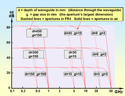
Figure 4AV Some estimated waveguides-below-cutoff, in air and FR4
When the frequency to be shielded is above 1GHz, the apertures in the shield will usually need to be less than 3mm in air, or 1.5mm inside the PCB, and waveguide-below-cutoff techniques can be used without sacrificing too much PCB area.
In the pervious example of a shielding-can with an SE specification of 20dB at 3GHz, we had a problem with the spacing of the through-holes that provide the electrical bonds between the plane layer (or guard trace) on the top surface of the PCB and the plane layer that provides the sixth side of the shielding-can. If the vertical spacing between the planes (or guard trace and plane) was 1.6mm and we used a 1mm spacing laterally between the via holes, the diagonal of the resulting apertures would be about 2mm, giving a cutoff frequency around 37.5GHz (assuming a 50% velocity of propagation inside the PCB) - well beyond the 3GHz we are concerned about.
A 6mm overlap between the top plane (or guard trace) and the inner plane would achieve an SE of about 81dB for each aperture at 3GHz. The 50mm side of the shielding-can requires 50 of these 1mm wide apertures, and this quantity would reduce their overall SE by about 34dB to about 47dB. Compared with the 20dB SE specification this is a very good figure, showing how effective the waveguide-below-cutoff technique can be.
Note that the waveguide-below-cutoff created by the plane (or guard trace) on the top surface plus the layer providing the sixth side of the shielding-can, can extend inside or outside its wall, or lie partially inside or outside.
As well as the waveguide-below-cutoff technique being used inside the PCB, it can be used to reduce the effects of apertures in the rest of the shield can. It is important to note that no conductor should be routed through a waveguide-below-cutoff aperture - to do so would reduce its SE to zero.
4.4.8 Cavity resonances in PCB shielding-cans
Resonances (standing waves) can occur within the cavity formed by a shielding-can at frequencies at which whole numbers of half-wavelengths will fit between its sides. They can be calculated (in GHz) by: f = 150 √{(l/L)2 + (m/W)2 + (n/H)2} - where: l, m, n are integers (0, 1, 2, 3, etc.) and L, W, H are the shielding-can’s length, width, height (in millimetres). Usually we are most interested in the lowest resonant frequency of the longest dimension, its ’3-D diagonal’, when: l = 1, m = 1, and n = 1 (the ’1,1,1 mode’), when a 50 by 30 by 5mm shielding-can will resonate at its lowest resonant frequency at 2.56GHz. The 1,0,0 (lengthwise) and 0,1,0 (widthwise) modes for the same can occur at 3GHz and 5GHz.
Resonances inside shielding-cans cause local amplification of their internal E and H fields at ’hot spots’ within the shielding-can, and these increase the coupling between circuits covered by the same shielding-can. Figure 4AW shows the coupling measured inside one shielding-can [33] [34].
Also, the SE of a shielding-can is reduced at its internal resonant frequencies, with 20dB reduction being recorded by [33] [34]. This reduction in SE appears to be due to locally intense fields (hot spots) being near to apertures and conductor penetrations, causing them to leak more. Figure 4AX shows the SE of the same shielding-can that was measured for Figure 4AW.
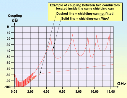
Figure 4AW Effects of cavity resonances on crosstalk inside a PCB shielding-can, from [33] and [34]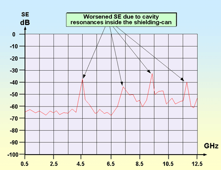
Figure 4AX Effects of cavity resonances on the SE of a PCB shielding-can, from [33] and [34]
So it is best to use shielding-cans that have length and width dimensions much smaller than half a wavelength at the highest frequency of concern, to prevent internal resonances from occurring in the frequency range concerned. Multiple shielding compartments can be formed in one shielding-can component to increase the resonant frequencies in each compartment to well beyond the highest frequency of concern, and also to help reduce interaction (crosstalk) between circuits [34].
Figure 4AS shows an example of a multi-compartmented PCB shielding-can, and Figure 4AY shows some more. Laird Technologies have developed a ’mold-in-place’ elastomer rib that they claim makes PCB-mounted shields much more effective and easy to assemble. The left hand side of Figure 4AY shows an example of a double-sided shielding-can assembly for a cellphone (using microvia technology as shown in Figure 4AR but without soldering the cans to the PCB).
The PCB of the cellphone shown in exploded view has a number of guard traces on each side, which align with the perimeter of the multi-compartmented shielding-cans and also with their internal metal dividers. The shielding-cans are located in moulded features in the plastic case halves, as is the PCB. When the case halves are clipped together everything automatically aligns and the ’mold-in-place’ conductive elastomer ribs make contact with the guard traces. Very easy assembly, and very easy to dismantle for recycling too.
The right hand side of Figure 4AY shows a similar multi-compartmented PCB shielding-can and a PCB with perimeter guard traces following the internal and external walls of the can, and ’mold-in-place’ gaskets on the can walls, but this one is clipped onto the PCB by means of its protruding metal fingers. These fingers clip into small slots routed in the PCB, but do not make any electrical connections. As for the cellphone on Figure 4AY, assembly is simply a question of pressing the parts together, and disassembly is easy.
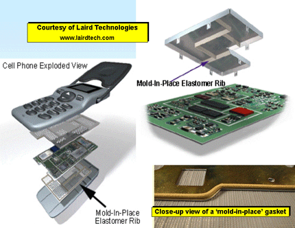
Figure 4AY Examples of multi-compartmented shielding-cans that are simply clipped into place
If it is not practical to avoid shielding-cans that are resonant within the frequency range of concern, then square (and cube) shaped structures should be avoided - as should structures with simple relationships between length, width and height (for example: 3:2:1). This is because at some frequencies such shapes will suffer from resonances due to their length and width together (or any two or three of the dimensions L, W and H). The amplification of internal fields at hot spots at these frequencies will be especially intense, and more likely to lead to undesirable results.
Ratios between L, W and H should ideally be irrational numbers, such as π (1.414..etc.) or preferably the ’Golden Mean’ (1.618..etc.), to help prevent coincidence of resonances. It will also help if the opposing sides of the shielding-cans are not parallel, but this technique is not often used, maybe because it does not result in a very pleasing appearance for a PCB assembly.
Another useful technique where cavity resonances in a shielding-can are potential problems is to use microwave-absorbing materials, such as Q-Zorb from Laird Technologies [36]. These are elastomers loaded with ferrite particles, usually a millimetre or two thick, glued to the inside of the lid of a shielding-can. These convert H fields into heat, thereby damping down both the E and H field resonances within the shielding-can.
4.4.9 Shielded cables and traces entering/exiting PCB shielding-cans
As discussed in 2.2.2 of [4], fibre-optics can be much more cost-effective, overall, than conductive interconnections when EMC issues are taken into account. Their transmitters and receivers need to be shielded, but they are only small components, as shown in Figure 4AZ.
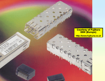
Figure 4AZ Fibre-optic transmitter/receivers with integrated PCB shielding-cans
But if conductors are used to connect to a circuit under a PCB shielding-can - for the can’s SE not to be degraded, all of the conductors penetrating its boundaries must either be RF-bonded, filtered or shielded, according to the principles discussed in 4.3.17 above.
Where shielded PCB traces enter or exit a shielded area of PCB, they must be routed as striplines between two plane layers that bond to all of the via holes in the guard trace around the perimeter of the shielding-can. The two plane layers must be electrically bonded together with plated-through via holes, and it is recommended that these vias should be no more than λ/30 apart (for example, no more than 10mm for frequencies less than 1GHz), preferably much closer.
Where a shielded cable enters or exits a PCB shielding-can, its connector or gland must make a direct electrical connection all around the perimeter of its aperture in the shielding-can, and also all around the perimeter of the cable’s shield. This is often called 360ø shield bonding, and is best done using circular connectors, or rectangular connectors with conductive gaskets, as discussed in 2.6.5 - 2.6.7 of [4].
Unfortunately, many of the connectors associated with ’modern’ digital data interconnections, such as RJ11, RJ45 (see Figure 4AP), USB2.0, Firewire, etc., use cheap folded metal bodies which have seams in them, so are not as good as deep-drawn types. They are also rectangular types but instead of conductive gaskets they most often use multi-point bonding with a few little bits of bent metal. As a result of their generally cheap (and nasty) design their effect on the SE of an enclosure, whether at product or PCB-level, is generally quite poor. However, a few manufacturers offer types with improved SE characteristics, and they are well worth buying.
A very interesting result of all the above is that it is easy to make a fully shielded PCB assembly, using plane layers on the top and bottom of the PCB, stitched together with a ’via wall’ all around the perimeter of the PCB, with shielding-cans fitted over all of the exposed devices and traces. An example is shown in Figure 4BA.
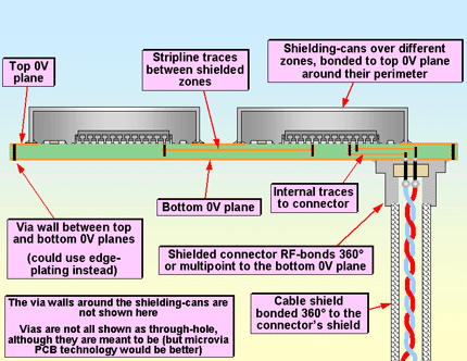
Figure 4BA Example of a fully-shielded PCB assembly
If you were to look at the component side of the assembly shown in Figure 4BA, you would only see metal - either the metal of the tops of the shielding-cans, or the metal of the top-side 0V plane. The top-side 0V planes are actually extensions of the guard traces, so are RF-bonded to the perimeter of each can using solder, conductive gaskets (see Figure 4AZ), or multipoint spring fingers.
4.4.10 Combining filtering with shielding at PCB level
Where a conductor entering or exiting a PCB shielding-can is filtered, the best performance is achieved with feedthrough filters. To avoid the high cost of their manual assembly and wiring, three-terminal surface-mounted filters are used instead, and their performance is optimised by locating them on the PCB so that their centre terminals align with - and are soldered to - the guard trace that is routed around the perimeter of the shielding-can. In this way, their input and output terminals lie either side of the shield - and are shielded from each other.
Leaded feedthrough filters are screwed or soldered into appropriately dimensioned holes in the shielding-can. But SMD types lie flat on the PCB and protrude through small apertures in the bottom edge of the shielding-can’s wall, as shown in Figure 4AP. The holes cut into the walls of the can for the three-terminal SMD filters to pass through are known as ’mouseholes’ (for reasons that should be obvious to anyone familiar with ’Tom and Jerry’ cartoons). The performance of the three-terminal SMD filters will be improved if the 0V plane via holes and shielding-can connection points to the guard trace are symmetrically placed with respect to the body of the filter component.
For more detail on using filtering in conjunction with shielding, including an example PCB pad pattern and graph showing how the performance of PCB-mounted filters is improved dramatically at frequencies above 100MHz, see 3.3.3 and 3,3,4 in [3].
Figure 4BB sketches the construction of a PCB assembly that is shielded and filtered. In some circumstances such an assembly might not need any further EMC measures, apart from a plastic box or other means to prevent electrostatic discharges occurring directly to its unshielded components.
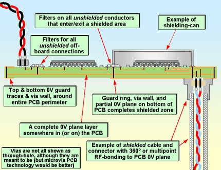
Figure 4BB Example of a partially-shielded PCB assembly, with filtering of traces and cables
Sometimes adequate EMC performance can be achieved solely by the use of the filters or shielding-cans. It may be worthwhile experimenting, during EMC testing [37], with lower-cost three-terminal filters, feedthrough capacitors, ferrite beads, or even zero-ohm links - so it helps to ensure that the pad patterns for the filters will accommodate a variety of such devices.
4.4.11 Combing heatsinking with shielding at PCB level
Some modern ICs dissipate significant amounts of heat and so require heatsinking. Where PCB-level shielding is also required, shielding-cans are combined with heatsinks. The metal base of the heatsink becomes the lid of the shielding-can, so the shielding-can on its own is little more than a four-sided shielding wall - with its bottom face completed by a PCB plane layer - and its top face completed by the base of the heatsink. Figure 4BC sketches an example.

Figure 4BC Example of combining heatsinking and shielding for an IC
The base of the heatsink must have a highly conductive surface using metals chosen so that they will not corrode after years of contact with the shielding wall. The heatsink is usually not soldered to the shielding wall (although this could be done under certain circumstances). Normally, all the various ’pressure sensitive’ techniques that can be used for attaching shielding-can walls to PCBs can also be used to electrically bond the walls to the base of the heatsink. The spacing rules for the electrical bonds to the heatsink are the same as those (above) for bonds to PCB planes.
Figure 4BD shows an example of an Intel-designed shield for one of their ICs. It has metal tabs for soldering to the PCB’s guard trace, and spring fingers on its top surface for multipoint RF-bonding to the base of the heatsink. The same figure also shows a spring-finger style ’picture frame’ shield into which can be clipped a heatsink.
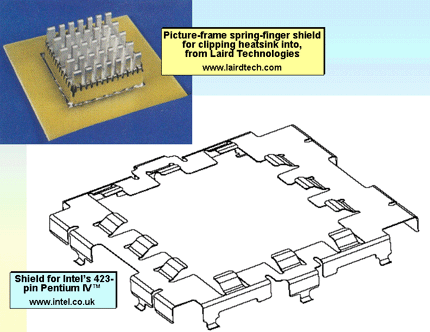
Figure 4BD Examples of commercially-available parts for combining shielding with heatsinks
4.5 Estimating shielding effectiveness with PC-based simulators
The only really sensible way to discover the SE of any complex enclosure with apertures is to model the structure, along with any PCBs and conductors (especially those that might be near any apertures) with a 3-dimensional field solver. Software packages that can do this now have more user-friendly interfaces and run on desktop PCs, alternatively there are some bureau services and universities that have the necessary software (and the skills to drive it so as to get reasonably accurate results).
There are some free SE calculators on the Internet that can help estimate the effects of a few apertures on the far-field SE of simple rectangular enclosures, for example [15] and [16]. But PC-based 3-D field solvers are necessary for reasonably accurate predictions of SE, for multiple apertures, dissimilar aperture shapes/sizes, aperture spacings > λ/4, complex enclosure shapes and conductor penetrations, in both the near-field and far-field, for example FLO/EMC from Flomerics.
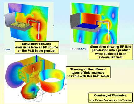
Figure 4BE Examples of shielding simulations using FLO/EMC
Without field-solving, the best bet for any reasonable accuracy is to mock-up the actual construction as well as can be done, plus the internal electronics or whatever, and test its SE in an EMC test laboratory at the earliest stage in a project to avoid unpleasant surprises later on. Various methods exist for SE testing of enclosures, although few of them are standardised. It is possible to do tests without using an EMC test laboratory, for instance using close-field probes you can make yourself (see Parts 1, 2 and 4 of [19]), or desk-top strip-line testers such as those made by Richard Marshall Ltd (www.design-emc.co.uk).
Since SE will vary strongly with the method and quality of assembly, materials, and internal PCBs and cables, it is always best to allow an SE ’safety margin’ of 20dB, or at least design-in features that will allow SE to be improved by at least 20dB if emissions/immunity problems are experienced during EMC testing of the final design. The small amount of extra time required during the early design stages will be more than amply rewarded by the reduction in financial risk at a later stage in the project (see Chapter 1 of [22]).
4.8 References
[1] Keith Armstrong, "Design Techniques for EMC", UK EMC Journal, a 6-part series published bi-monthly over the period February - December 1999. An improved version of this original series is available from the "Publications & Downloads" page at www.cherryclough.com
[2] The Institution of Engineering and Technology (IET, was the Institution of Electrical Engineers, IEE), Professional Network on Functional Safety, "EMC and Functional Safety Resource List", from the "Publications & Downloads" page at www.cherryclough.com
[3] Keith Armstrong, "Design Techniques for EMC, Part 3 - Filtering and Suppressing Transients", The EMC Journal, September and November 2006, and January 2007, from the EMC Journal archives at www.compliance-club.com.
[4] Keith Armstrong, "Design Techniques for EMC, Part 2 - Cables and Connectors", The EMC Journal, May and July 2006, from the EMC Journal archives at www.compliance-club.com.
[5] John R Barnes, "Robust Electronic Design Reference Book, Volume I", Kluwer Academic Publishers, 2004, ISBN: 1-4020-7737-8. See Chapter 34 for shielding and shielding design.
[6] Keith Armstrong, "Design Techniques for EMC, Part 0 - Introduction, and Part 1 - Circuit Design and Choice of Components", The EMC Journal, January 2006 pp 29-41, plus March 2006 pp 30-37, available from http://www.compliance-club.com.
[7] "Shielding Design and Calculation", Ron Brewer, Laird Technologies Tech Notes #105, from www.lairdtech.com
[8] RF Caf‚, Skin Depth, http://www.rfcafe.com/references/electrical/skin_depth.htm
[9] "Shielding Methods", Chomerics, http://www.chomerics.com/tech/Shielding_methods.htm
[10]"EMI Shielding Engineering Handbook", Chomerics, available from: http://www.chomerics.com/tech/Shielding_methods.htm
[11]The chapter entitled "EMI Shielding Theory & Gasket Design Guide" in the Chomerics "EMI Shielding Engineering Handbook", available from: http://www.chomerics.com/products/emi_lit_contents.htm
[12]"Technical Notes", Laird Technologies, technical information and guidance on shielding and gasketting, available from: http://www.lairdtech.com/pages/catalogs/emi.asp (scroll down the page to the "Technical Notes" section).
[13]William A. Radasky, "The Threat and Detection of Electromagnetic Weapons at Airports and on Aircraft", 2005 IEEE Conference on Technologies for Homeland Security, Boston, Massachusetts, 26 April 2005, available from http://.ieeexplore.ieee.org
[14]"An Aperture Attenuation Modeling Program to Determine Shielding Effectiveness of Printed Circuit Board Shields and Other Enclosures", free spreadsheet from MAJR Products, Inc., download from http://www.majr.com/freetool.htm
[15]A free SE calculator (for far-field SE): www.emc.york.ac.uk/examples/screening/index.html
[16]A free SE calculator (for far-field SE): http://www.amanogawa.com/index.html (click on 'EMC/EMI', then 'Java Applets', then on 'Shielding Effectiveness')
[17]Shabista Ali, Daniel S Weile, Thomas Clupper, "Effect of Near Field Radiators on the Radiation Leakage Through Perforated Shields", IEEE Transactions on EMC, Vol 47, No. 2, May 2005, pp 367-373.
[18]Keith Armstrong, "Design Techniques for EMC, Part 3 - Filtering, and Suppressing Transients", The EMC Journal, September and November 2006, January 2007, available from http://www.compliance-club.com.
[19]Tim Williams and Keith Armstrong, "EMC Testing", a series in seven parts published in the EMC & Compliance Journal 2001-2, available from the 'Publications & Downloads' page at www.cherryclough.com.
[20]Keith Armstrong, "Design Techniques for EMC Part 4 - Shielding (Screening) first half", The EMC Journal, March 2007, pp 31-46, www.compliance-club.com
[21]M K Armstrong, "GigaHertz Shielding at Printed Circuit Board Level - Eliminate or Reduce Enclosure Shielding Costs", IEE "New EMC Issues in Design" event held at Qinetiq, 28th April2004.
[22]Keith Armstrong, "EMC for Printed Circuit Boards (PCBs) - Basic and Advanced Design Techniques", Armstrong/Nutwood UK Ltd. January 2007, view details at http://www.cherryclough.com, order from pam@nutwood.eu.com
[23]The basic standard on microvia PCB technology is IPC-2315, from the Institute of Printed Circuits at www.ipc.org.
[24]Steve Owen, "The Shielding Effectiveness of In-Mould Labelled Enclosures", EMC York 2000 Conference, 10-11 July 2000<br />
[25]Chris Hills, "Formed EMI Shields, the Green Replacement for Conductive Paint and Plating for Plastic Housings", EMC Compliance Journal, June 2000, pp 36-39
[26]Maria Sabrina Sarto et al, "New Light-Weight Formable Shields", EMC Compliance Journal, Aug. 2001, pp 17-19
[27]Maria Sabrina Sarto et al, "An Innovative Shielding Concept for EMI Reduction", IEEE EMC Society Newsletter, Summer 2001, Issue No. 190, pp 22-28
[28]"EMC Shielding with Carbon Fibres", IEE EMC Professional Network, EMC Industry News 2002-11-21
[29]Jack Black, "Automated Installation of Surface Mountable EMI Shields Using Tape and Reel Packaging", BMI Inc., Palatine, IL, USA
[30]Darryl Yarborough, "EMI Shield Mounting Methods, Some Tried and Some New, Through-Hole, Surface, and the New Hybrid", Conformity, Jan. 2001, pp 32-34
[31]Gore-Shield GS5200 Gaskets, www.gore.com
[32]Roy Bjorlin, Gary Shawhan, "Conformal Board-Level Shielding Products", Interference Technology Annual Guide 2003, pp 226-230
[33]Thomas Clupper, "Improve PCB Shielding for Portable Devices", Microwaves and RF, May 2003, pp 72-84
[34]Thomas Clupper, "A New PCB-Level Shielding Technology", Interference Technology Annual Guide 2003, pp 187-195
[35]Eisuke Hanada et al, "Electromagnetic Attenuation with Stainless-Steel Fiber Mesh", IEEE EMC Society Newsletter, 2003
[36]Laird Technologies, www.lairdtech.com. To access their "Knowledge Base", click on "Technical Resources".
[37]Tim Williams and Keith Armstrong, "EMC Testing", a series of seven articles in the EMC & Compliance Journal, Feb 2001 - Apr 2002, www.compliance-club.com/KeithArmstrongPortfolio
[38]Rocky R Arnold, "Electronic Product Trends Drive New EMI/RFI Shielding Solutions", Interference Technology, EMC Test and Design Guide 2003, pp 48-53
[39]J P Quine, A J Pesta, "Shielding Effectiveness of an Enclosure Employing Gasketted Seams - Relation between SE and Gasket Transfer Impedance", IEEE 19995 International Symposium on EMC, Atlanta, 14-18 August 1995, ISBN: 0-7803-2573-7, pp 392-395, available via http://ieeexplore.ieee.org
[40]Gary Fenical,"Ten Considerations When Specifying an RF Gasket", Interference Technology, EMC Test & Design Guide 2005, pp 64-72, www.interferencetechnology.com
[41]Ed Nakauchi and Mike Oliver, "EMI Shielding with Thermal Management", EE - Evaluation Engineering, August 2002, www.evaluationengineering.com
[42]W Drew Perigrim, "Plating to Obtain Maximum Shielding Performance", Laird Technologies Tech Notes #103, from www.lairdtech.com
[43]Richard A Anderson, "Reviewing RoHS Compliance for Harsh Environments", Microwaves & RF, February 2007, pages 66-75. www.mwrf.com.
[44]NAVAIR AD 115 "Electromagnetic Compatibility Design Guide for Avionics and Related Ground Equipment", 3rd Edition June 1988, Naval Air Systems Command, Department of the Navy, Washington DC, USA. This document does not appear to be easily obtainable via the Internet, and has probably been superseded by a more recent US military standard.
[45]John R Barnes, "Robust Electronic Design Reference Book, Volume II, Appendices", Kluwer Academic Publishers, 2004, ISBN 1-4020-7738-6
4.9 Acknowledgements
I am very grateful to the following people for suggesting a number of corrections, modifications and additions to the first series published in 1999 [1]: Feng Chen, Kevin Ellis, Neil Helsby, Alan Keenan, Mike Langrish, Tom Liszka, Tom Sato, and John Woodgate.
Eur Ing Keith Armstrong CEng MIEE MIEEE
Partner, Cherry Clough Consultants, www.cherryclough.com, Member EMCIA
Phone: +44 (0)1785 660 247, Fax: +44 (0)1785 660 247, keith.armstrong@cherryclough.com
www.cherryclough.com